
Basic Circuit
Index 299
ZERO_SUPPRESSION
Published:2009/7/1 20:52:00 Author:May

Simple CMOS circuit using MC14011 quad two-input NAND gate and MC14558 IC provides zero suppression for multiplexed displays in which scanning is left to right for leading-zero suppression and right to left for trailing zeros. Article covers operation of circuit.-J. J. Roy, Eliminate Excess Zeros in Multiplexed Displays, EDN Magazine, Sept. 5, 1975, p 77. (View)
View full Circuit Diagram | Comments | Reading(1739)
TACHOMETER_USING_MAGNETIC_PICKUP_
Published:2009/7/1 20:51:00 Author:May

Signal frequency proportional to shaft speed being measured is fed into National LM2907 IC for conversion to output voltage that is proportional to input frequency. Output is zero at zero frequency. Ouality of timing capacitor C1 determines accuracy of unit over temperature range.Use equivalent zener-regulated LM2917 IC if output voltage must be independent of variations in supply voltage.- Linear Applications, Vol. 2, National Semiconductor, Santa Clara, CA, 1976, AN-162, p 3-4. (View)
View full Circuit Diagram | Comments | Reading(2193)
SCA_Background_Music_DECODER
Published:2009/7/1 20:37:00 Author:May

A resistive voltage divider is used to establish a bias voltage for the input (Pins 2 and 3). The demodulated (multiplex) FM signal is fed to the input through a two-stage high-pass filter, both to effect capacitive coupling and to attenuate the strong signal of the regular channel. A total signal amplitude, between 80 mV and 300 mV, is required at the input. Its source should have an impedance of less than 10,000 ohm. The Phase-Locked Loop is tuned to 67 kHz with a 5000 ohm potentiometer, only approximate tuning is required since the loop will seek the signal. The demodulated output (Pin 7) passes through a three-stage low-pass filter to provide de-emphasis and attenuate the high-frequency noise which often accompanies SCA transmission. Note that no capacitor is provided directly at Pin 7; thus, the circuit is operating as a first-order loop. The demodulated output signal is in the order of 50 mV and the frequency response extends to 7 kHz. (View)
View full Circuit Diagram | Comments | Reading(1546)
WHO_IS_FIRST
Published:2009/7/1 20:35:00 Author:May
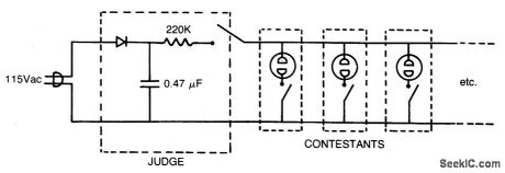
Circuit Notes
Here is a circuit for any question-and-answer party game. The first button pushed ionizes the neon bulb dropping the dc voltage on the parallel neons (the other contestants) below the ionization level: determining unequivocally the first person to press the button. (View)
View full Circuit Diagram | Comments | Reading(467)
ANALOG_MEMORY
Published:2009/7/1 20:35:00 Author:May
Used in synthesizer for generating wide variety of musical and other sounds, to provide constant control signal for sounds requiring long fadeout. Positive input pulse initiates sampling of analog signal for pre-set time, with signal being held for unspecified period. Input voltage range is from about -0.5 V to +6.5 V, being deliberately limited by D1 Three-part article describes operation in detail and gives all other circuits used in synthesizer.-T. 0rr and D. W. Thomas, Elec-tronic Sound Synthesizer, Wireless World, Part 3-Oct. 1973, p 485-490 (Part 1-Aug. 1973, p 366-372; Part 2-Sept. 1973, p 429-434). (View)
View full Circuit Diagram | Comments | Reading(663)
FREQUENCY_DIVISION_MULTIPLEX(FDM)STEREO_DECODER
Published:2009/7/1 20:33:00 Author:May
View full Circuit Diagram | Comments | Reading(2529)
MICROPOWER_MONO
Published:2009/7/1 19:54:00 Author:May
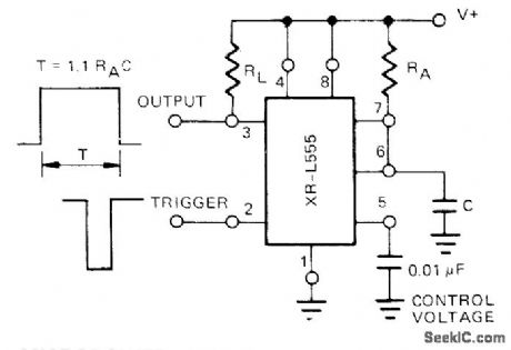
Uses Exar XR-L555 having typical power dissipation of only 900 μW at 5 V, serving as direct replacement for 555 timer in micropower circuits. Time delay is con-trolled by one external resistor and one capacitor (RA and C) which determine output pulse duration. Can be triggered or reset on falling waveform. Output will drive TTL circuits or source up to 50 mA.- Timer Data Book, Exar Integrated Systems, Sunnyvale, CA, 1978, p 7-8. (View)
View full Circuit Diagram | Comments | Reading(579)
HIGH_PRECISION_F_V
Published:2009/7/1 20:26:00 Author:May
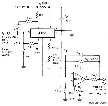
Use of integrator opamp with frequency-to-voltag e connection of RM4151 converter gives increased accuracyand linearity for converting square-wave inputs of 0-10 kHz to proportional output voltage in range of -10 V to 0 V.- Linear Integrated Circult Data Book, Raytheon Semiconductor Division, Mountain View, CA, 1978, p 7-39. (View)
View full Circuit Diagram | Comments | Reading(523)
VOLTAGE_CONTROLLED_MONO_1
Published:2009/7/1 20:25:00 Author:May

Circuit gives choice of Linear sawtooth and constant pulse-width outputs over frequency range from DC to 50 kHz. Output frequency and pulse repetition rate vary linearly with control current. Applications include audio synthesizers, variable time bases, and current-to-frequency converters.-S. Wetenkamp, Minor Changes Turn VCO into Voltage-Controlled One-Shot, EDN Magazine, March S, 1978, p 67-69. (View)
View full Circuit Diagram | Comments | Reading(1963)
MOSFET_ASTABLE
Published:2009/7/1 20:24:00 Author:May
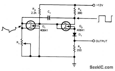
RCA 40841 dual-gate N-channel depletion-type MOSFETs alternate between high and low conduction states in between dormant periods when C1 is charging or discharging through R1 Circuit switches state when voltage level at gate of a, makes gain lf high enough for regeneration to occur. D1 reduces voltage across R4 to give TTL drive capability.-D. R. Armstrong, Wide-Frequency Astable Multivibrator Uses One R-C Network, EDN Magazine, Aug, 5, 1977, p 54. (View)
View full Circuit Diagram | Comments | Reading(2198)
UJT_MONO
Published:2009/7/1 20:23:00 Author:May
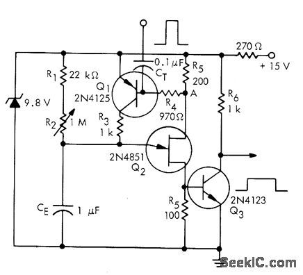
UJT Q2 is normally on, with its emitter saturation current supplied by transistor Q1 which is also on. Application of positive trigger pulse to base of a, turns both off to start timing cycle. CE starts charging each time from saturation voltage of UJT. When capacitor voltage becomes high enough to fire UJT, Q1 turns on and supplies emitter current required to keep UJT on. Output transistor a, delivers pulse having duration related to value used for CE.- Unijunction Transistor Timers and Oscillators, Motorola, Phoenix, AZ, 1974, AN-294 p 5. (View)
View full Circuit Diagram | Comments | Reading(723)
PRECISION_MONO
Published:2009/7/1 20:19:00 Author:May

Negative-going pulse triggers mono, making output go LOW for duration of eight clock pulses at frequency determined by values of R and C in 4011 clock generator IC1. R1 is greater than 2RT, and clock frequency is 1/13.8RTC. Width of output pulse depends on number of stages in shift register IC, and clock frequency.-B. Bong, Two CMOS IC's Yield Precision One-Shot, EDN Magazine, Aug. 5, 1978, p 82. (View)
View full Circuit Diagram | Comments | Reading(695)
DIRECT_COUPLED_ASTABLE
Published:2009/7/1 20:14:00 Author:May
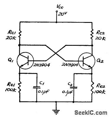
Collectors and bases of both emitter-biased transistors are directly coupled to each other. Switching action takes place by means of capacitor in each emitter circuit. Triangle waves are generated at emitters. Neither transistor can remain permanently cut off. Instead, circuit has two quasi-states, with switching action achieved by charging and discharging capacitor between these states. Single 0.1-μF capacitor can be used between emitters in place of C1 and C2.-S. Chang, Two New Direct-Coupled Astable Multivibrators, Proceedings of the IEEE, March 1973, p 390-391. (View)
View full Circuit Diagram | Comments | Reading(543)
CLOCK_SYNCHRONIZED
Published:2009/7/1 20:14:00 Author:May
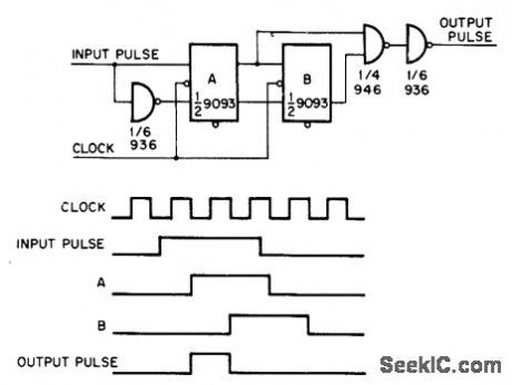
Circuit generates pulse that is two clock pulses wide, in synchronism with clock, from random input pulse whose width is more than 5 times that of clock pulse.
Flip-flops A and B are connected as shift register. When clock pulse falls, input of flip-flop A goes to 1 and sets it. B follows state of A with delay of one clock pulse. Output pulse can occur only once during a particular input strobe.-F. E. Nesbitt, Synchronized One Shot, EDN|EEE Magazine, May 15, 1971, p 50. (View)
View full Circuit Diagram | Comments | Reading(695)
GATED_PULSE_DESCRAMBLER
Published:2009/7/1 20:13:00 Author:May
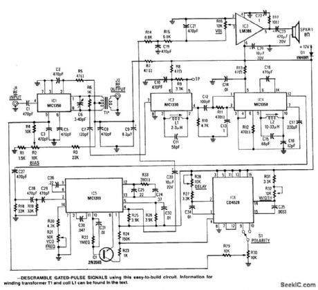
This circuit consists of an amplifier and video detector with a second subcarrier detector for synch recovery purposes. A pulse-former circuit modulates the gain of the main channel increasing it during synch intervals. Provision for subcarrier audio descrambling is also provided. Kit available from North Country Radio, P.O. Box 53, Wykagyl Station, New York 10804. (View)
View full Circuit Diagram | Comments | Reading(1531)
17_Hz_SQUARE_WAVES
Published:2009/7/1 20:13:00 Author:May
Uses three comparators from MC3302P IC to generate three sym-metrical square waves 120° apart. Inverting out-puts of comparators gives waves 60° apart. Operating voltage can be anywhere from 4 to 12V.-L,J. Bell, Three Coupled Astables, Wire-less World, Feb. 1977, p 44. (View)
View full Circuit Diagram | Comments | Reading(473)
PERFECT_SOUARE_WAVES_FORLAB
Published:2009/7/1 20:12:00 Author:May
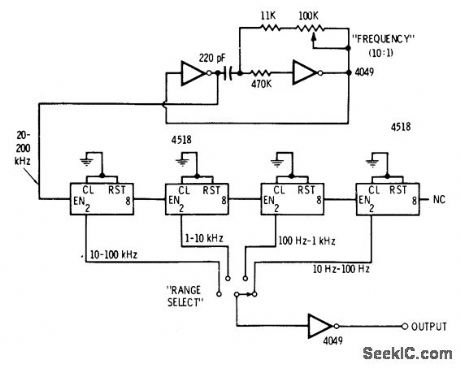
Two sections of 4049 hex inverting buffer are connected as 10:1 variable-frequency astable MVBR to feed chain of four divide-by-10 counters using 4518 dual counters. Frequency division pro-vides perfect symmetry for square-wave out-put.-D. Lancaster, CMOS Cookbook, Howard W. Sams, Indianapolis, IN, 1977, p 232-234. (View)
View full Circuit Diagram | Comments | Reading(716)
BASIC_MONO
Published:2009/7/1 20:11:00 Author:May
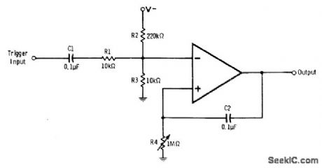
Opamp is normally in positive saturation because of negative voltage pro-vided by voltage divider R2-R3. When 2-V positive trigger pulse is applied to input, output of opamp swings into negative saturation but automatically returns to positive saturation after time interval determined by values used for C2 and R4. With R4 set at maximum resistance, this time is about 1 s. Increase size of C2 for longer time periods. Opamp can be 741 or equivalent.-R. Melen and H. Garland, Under-standing IC Operational Amplifiers, Howard W. Sams, Indianapolis, IN, 2nd Ed., 1978, p 120-121. (View)
View full Circuit Diagram | Comments | Reading(550)
MONO_WITH_NORMALLY_ONLED
Published:2009/7/1 20:10:00 Author:May
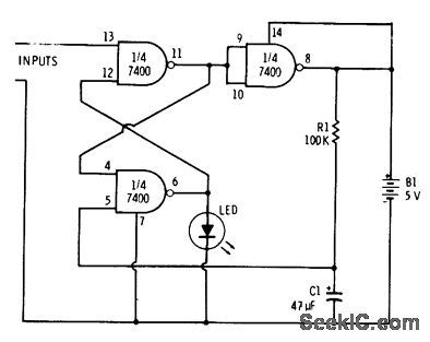
Connection shown for three gates of 7400 quad NAND gate inverts operating mode, so LED is normally on. Trigger pulse at input extinguishes LED for time determined by R1 and C1 while making gates change states. Gates revert to original states after delay also determined by values of R1 and C1.-F. M. Mims, Integrated Circuit Projects, Vol. 2, Radio Shack, Fort Worth, TX, 1977, 2nd Ed., p 19-26. (View)
View full Circuit Diagram | Comments | Reading(513)
IC_FLIP_FLOP_DEMONSTRATOR
Published:2009/7/1 20:09:00 Author:May

Demonstration circuit using RS7473 dual flip-flop incorporates 555 clock circuit providing sequential train of input pulses at AF rate to JK master slave flip-flop section for toggling LED loads of flip-flop back and forth between ON and OFF states. R1 controls rate at which LEDs flash on and off. Circuit is designed for Radio Shack 276041 or equivalent red LEDs. If clock is omitted, state of flip-flop is changed by grounding clock input pin 1 momentarily.-F. M. Mims, Integrated Circuit Projects, Vol. 6, Radio Shack, Fort Worth, TX, 1977, p 23-32. (View)
View full Circuit Diagram | Comments | Reading(5788)
| Pages:299/471 At 20281282283284285286287288289290291292293294295296297298299300Under 20 |
Circuit Categories
power supply circuit
Amplifier Circuit
Basic Circuit
LED and Light Circuit
Sensor Circuit
Signal Processing
Electrical Equipment Circuit
Control Circuit
Remote Control Circuit
A/D-D/A Converter Circuit
Audio Circuit
Measuring and Test Circuit
Communication Circuit
Computer-Related Circuit
555 Circuit
Automotive Circuit
Repairing Circuit