
Basic Circuit
Index 285
FAST_TTL_PROBE
Published:2009/7/2 22:56:00 Author:May
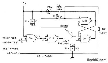
RS flip-flop wired from NAND gate detects pulses as short as combined gate delays of NAND sections forming flip-flop (about 30 ns). Circuit changes state at start of pulse, with LED monitoring flip-flop output.After pulse has been detected, circuit must be reset with S2. Will work with either positive-or negative-going pulse, as selected by S1.-W. A.Walde, Build a TTL Pulse Catcher, BYTE, Feb.1976, p 58 and 60. (View)
View full Circuit Diagram | Comments | Reading(958)
FM_MODULATOR_
Published:2009/7/2 22:53:00 Author:May
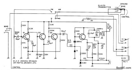
Developed to permit FM operation on AM transceiver. Consists of microphone preamplifier, driver amplifier, and 8-MHz crystal oscillator providing 24-MHz output.Audio from modulator drives variable-capacitance diode D1 (which can be silicon switching diode) in oscillator circuit. Adapter feeds AM transmitter in which frequency multipliers inGrease deviation to about 8.5 kHz,To reduce deviation for narrow-band FM,adjust 500K pot in preamρ.-R .Orozco,Jr.,Put That AM Rig on FM,73 Maga,April 1976,p 34-35. (View)
View full Circuit Diagram | Comments | Reading(906)
SIGAIAL_CONDITIONER
Published:2009/7/2 22:52:00 Author:May
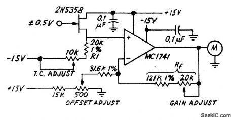
FET-buffered opamp circuit will operate from source impedances up to 100 megohms while providing voltage gain of 5. Offset adjustment is provided forinitial calibration of circuit. Developed for use with highimpedance sensors such as pH electrodes.- Industrial Control Engineering Bulletin. Motorola. Phoenix. AZ. 1973. EB-4. (View)
View full Circuit Diagram | Comments | Reading(547)
AUDIBLE_CMOS_PROBE
Published:2009/7/2 22:51:00 Author:May
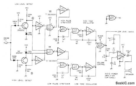
Eliminates need for watching meterwhile applying probe tip in turn to large number of closely spaced terminals during troubleshooting. Produces high tone for logic high, low tone for logic low, and no sound for open or floating string. Supplyis 12V.Articledescribes circuit operation in detaiL-C. W. An-dreasen, The Best Probe Yet?, 73 Magazine, April 1978, p 134-135. (View)
View full Circuit Diagram | Comments | Reading(562)
TTL_PROBE
Published:2009/7/2 22:46:00 Author:May


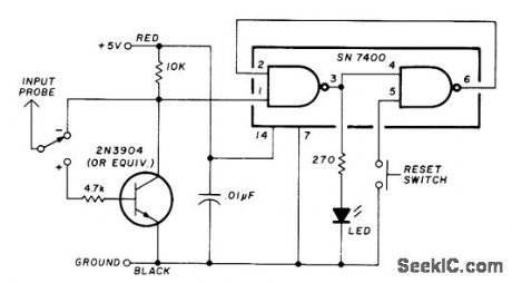
LED comes on, and stays on until circuit is reset, if input probe receives low-level (negative-going) pulse when polarity switch is set as shown. For other position of switch, LED comes on for high-level or+5 V pulse,-R .BShreve,Troubleshooting Logic Circuits,HamRadio.Feb 1977,p 56-59, (View)
View full Circuit Diagram | Comments | Reading(589)
VISUAL_AUDIBLE_PROBE
Published:2009/7/2 22:39:00 Author:May
Indication of static state of terminal in digital logic is made audible forblind experimenter by using NE556 timer IC3 as oscillator controlled by IC1 (SN74132N) and lC2 (SN7486N). Any logic transition from 1 to 0 or 0 to 1, lasting at least 50 ns, is detected and indicated by audio beep. Visual indication is provided by LED that comes on when input is logic 1.-T. Lincoln, A Logic Probe You Can Hear, 73Magazine, Aug. 1976, p 106. (View)
View full Circuit Diagram | Comments | Reading(638)
TUNER_USES_IC
Published:2009/7/2 22:37:00 Author:May

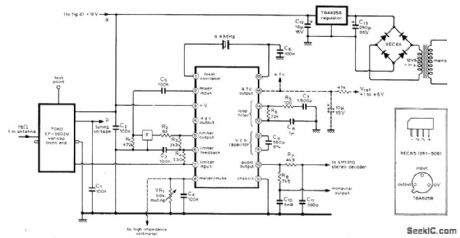

Availability of Signetics NE563 IC having about 180 transistors greatly simplifies construction of high-qualitiy FM tuner . IC includes circuits for converting IF output signal to lower frequency for driving phaselocked loop of demodulator . use of varicap front end permits switched or continuous Tuning with 100K Helipot or with switched preset 100k pots connected between +12 V and ground .tuning contorls can be remotely located .After 60 dB of amplification in NE563 IC,signal passes through ceramic filter F(Vernitron FM-4 or Toko CFS) before being fed back through C5 to IC for mixing with crystal -controlled 9.8-MHz local oscillator.Article covers construction and operation of tunner in detail.-J.B.Dance,High-Quanlity F.M.Tuner,Wireless World ,March 1975,p 111-113. (View)
View full Circuit Diagram | Comments | Reading(2196)
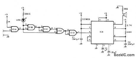
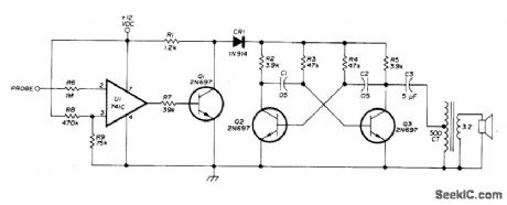
LISTEN_TO_LOGIC
Published:2009/7/2 22:34:00 Author:May


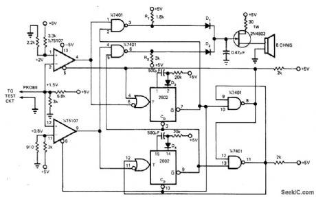
Gives audio indication of TTL states when probe is held on IC pin. Input level above 2 V makes 2N48O3 UJT oscillate at about 400 Hz and give tone from loudspeaker.Logic 0 at probe input gives lower frequency.Logic pulse transitions trigger 2602 dual monos for 1 s, modulating tones at about 1-s rate.Monos also drive two-gate latch that prevents either mono from firing two consecutive times.-I. Simon, Audio Output Eases Logic Level Checking, EDNMagazine, June 20, 1975, p 116and 118. (View)
View full Circuit Diagram | Comments | Reading(776)
1_kHz_BANDPASS_2
Published:2009/7/2 22:30:00 Author:May
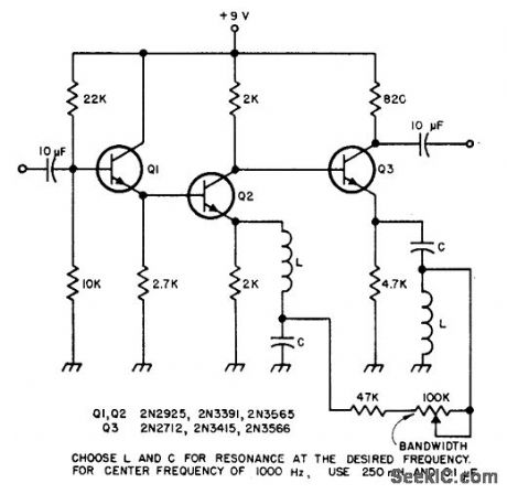
Three-stage audio filteruses two series resonant circuits to give very narrow audio passband Amount of feedback determines Q and bandwidth.-Circuits,Magazine, March 1974, p 89. (View)
View full Circuit Diagram | Comments | Reading(542)
CMOS_LOGIC_PROBE
Published:2009/7/2 22:29:00 Author:May

Designed for wiring into microprocessor to show status of an important terminal, as troubleshooting aid. LEVEL LED is on for TTL input of 1 and off for input of 0. EDGE LED lights momentarily when input changes from 1 to 0 or 0 to 1. Use of CMOS inverting buffer 3a at input prevents probe from affecting microprocessor.-F. A. Weissig, A CMOS Logic Probe, BYTE, Oct. 1977, p 11. (View)
View full Circuit Diagram | Comments | Reading(2115)
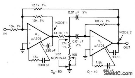
FASTER_SLEWING
Published:2009/7/2 22:18:00 Author:May

Single transistor stage at output of opamp increases slewing rate by factor equal to gain of transistor stage. Choose R1 to meet output impedance requirements and current rating of supply. R2 is then made equal to R1 divided by desired gain of transistor stage. Collector of Tr1 should be at 0 V when output of opamp is 0 V. assuming feedback loop is not closed by Rf. Article gives design equations.-L. Short. Faster Slewing Rate with 741 Op-Amp. Wireless World. Jan. 1973. p 31 (View)
View full Circuit Diagram | Comments | Reading(547)
PROBE
Published:2009/7/2 22:17:00 Author:May
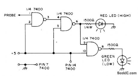
Red LED comes on to indicate thattest point is at high logic level, while green LED signifies low level. Circuit uses one 7400 quad dualinput NAND gate.-S. Uhrig, Check Logic with This Simple Probe, 73 fidagazine, Dee. 1974, p 76. (View)
View full Circuit Diagram | Comments | Reading(1922)
RECTIFIER_WITHOUT_DC_OFFSET
Published:2009/7/2 22:11:00 Author:May
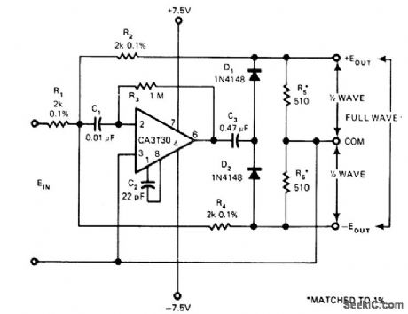
Avoids drawback ofJarge nonlinearity at low signal levels. by isolating AC of opamp from DC output.Circuit has wide bandwidth, as required for rectifying 20-kHz input signal with high precision, Output coupling capacitor C3 is low-Ieakage Mylar; for low-frequency operation. it can be replaced with two back-to-back low-leakage tantalums. D1 and D2 should be matched for forward voltage at peak load current. Use Hewlett-Packard 5082-2810 hot-carrier diodes instead to improve operation at millivolt signal levels or at higher frequencies.-D. Belanger. Single Op Amp Full-Wave Rectifier Has No DC Offset. EDN Magazine. April 5. 1977. p 144 and 146. (View)
View full Circuit Diagram | Comments | Reading(840)
AUDIBLE_LOGIC_INDICATOR
Published:2009/7/2 22:10:00 Author:May
Audio oscillator Q1-Q2-Q3 is isolated from TTL by opamp U1 wired as Schmitt trigger. Opamp acts as highinput-impedance inverter. Reference level is set at +1.6 V by R8-R9 for TTL-compatible logic (about midway between high and low logic levels). When probe input is below +1.6 V, opamp output of about 10.5 V saturates Q1and disables Q2-Q3 to cut off tone. When probe voltage is above +1.6 V, U1 output is about 2 V which cuts off Q1 and allows Q2-Q3 to generate tone indicating high logic.-H. F. Batie, Versatile Audio Oscillator, Ham Radio, Jan. 1976, p 72-74. (View)
View full Circuit Diagram | Comments | Reading(659)
20_dB_GAIN_FOR_2m
Published:2009/7/2 22:10:00 Author:May

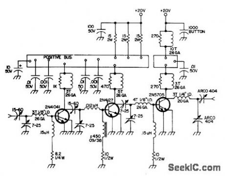
Input of 200 mW is amplified to 20 VV. Positive 20-V sources are separated so final stage can be amplitud-modulated; for FM, connect to single supply.Transistors require heatsinks.-Circuits, 73 Magazine, May 1973, p 106. (View)
View full Circuit Diagram | Comments | Reading(439)
SPEECH_RECOGNITION_FILTER
Published:2009/7/2 22:07:00 Author:May

Voice signal picked up by microphone is preamplified and sent through 3-kHz low-pass passive filter C1-R1 to 1-kHz high-pass active filter and 1-kHz low-pass active filter using sections of LM3900 quad opamp. Diode symbols on opamps indicate use of current mirrors for noninverting inputs. Outputs are sampled about 60 times per second to implement speech recognition algorithm of computer, which counts number of high-pass and low-pass zero crossings per second and compares results with series of word models in memory to determine most likely match.-J. R. Boddie, Speech Recognition for a Personal Computer System, BYTE, July 1977, p 64-68 and 70-71. (View)
View full Circuit Diagram | Comments | Reading(2358)
1_kHz_FIFTH_ORDER_LOW_PASS
Published:2009/7/2 22:06:00 Author:May

Uses single first-order section and two different second-order sections to give passband gain of 10.3 dB,Opamps can be 741 or equlvalent,-H,M.Berlin, Design of Active Filters, with Experments, Howard W,Sams, Indianapons, IN,1977,p 119-122. (View)
View full Circuit Diagram | Comments | Reading(957)
Q_MULTIPLlER
Published:2009/7/2 22:05:00 Author:May
Alticle glves design procedure and equations for utilking Q multiplication to simplify circuit for active bandpass filter,With values shown,center frequency is 3.6 kHz and Q of10 is multiplied by gain of 6 to give effective Q of 60.-A, B,Williams, Q-MultipIier Techniques Increase filtor Selectivity,EDN Magazine,Oct 5,1975,p74 and 76. (View)
View full Circuit Diagram | Comments | Reading(616)
TUNABLE_NOTCH_FILTER
Published:2009/7/2 22:03:00 Author:May

Simple pot-tuned active notch filter has tuning range of 200 Hz in audio band and 3-dB rejection bandwidth of 10 Hz, as required for tuning out whistle or powerline hum that is interfering with radio program.Article gives design theory for many other types of notch filters.-Y. Nezer, Activ (View)
View full Circuit Diagram | Comments | Reading(0)
TUNABLE_NOTCH
Published:2009/7/2 22:01:00 Author:May
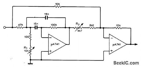
Opamp circuit requires only one pot (R1) to vary notch frequency. R2 is used to set noise rejection to maximum. With values shown, filter tunes from 170 Hz to 3 kHz, with 3-dB bandwidth of 230 Hz and notch rejection better than 40 dB over entire range. Circuit can be voltage-tuned by replacing R, with FET operated as voltage-variable resistor.-R. J.Harris, Simple Tunable Notch Filter, Wireless World, May 1973, p 253. (View)
View full Circuit Diagram | Comments | Reading(657)
| Pages:285/471 At 20281282283284285286287288289290291292293294295296297298299300Under 20 |
Circuit Categories
power supply circuit
Amplifier Circuit
Basic Circuit
LED and Light Circuit
Sensor Circuit
Signal Processing
Electrical Equipment Circuit
Control Circuit
Remote Control Circuit
A/D-D/A Converter Circuit
Audio Circuit
Measuring and Test Circuit
Communication Circuit
Computer-Related Circuit
555 Circuit
Automotive Circuit
Repairing Circuit