
Basic Circuit
Index 293
SQUIB_SIMULATOR
Published:2009/7/24 2:32:00 Author:Jessie

Simulates electrical characteristics of primer or squib of propellant-actuated fastener used in missiles and space systems for vehicle separation. Has very low impedance prior to firing, and infinite impedance after firing. Useful for testing firing circuits in laboratory where firing of actual squib would create disturbing sound.-C. S. Lewis, Electronic Squib Simulator, EEE, 10:9, p 24-25. (View)
View full Circuit Diagram | Comments | Reading(1289)
TIME_TO_VOLTAGE
Published:2009/7/2 3:15:00 Author:May

Time period of negative gating signal determines amplitude of linear output ramp generated by integrator opamp. Amplitude of ramp, proportional to input time, is observed on calibrated screen of oscilloscope.—G. B. Clayton, Experiments with Operational Amplifiers, Wireless World, Sept.1973, p 447-148 (View)
View full Circuit Diagram | Comments | Reading(719)
GENERATES_PREDETERMINED_NUMBER_OF_PULSES
Published:2009/7/24 2:31:00 Author:Jessie
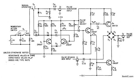
Provides group of pulses with fixed prr, at touch of switch S1, to simulate target returns of various radars. Number of output pulses depends on duration of gate, set by R8.-L. Turf, Simulator Circuit Generates Video or Noise Pulses, Electronics, 39:9, p 78-79. (View)
View full Circuit Diagram | Comments | Reading(517)
V_F_AND_F_V
Published:2009/7/2 3:15:00 Author:May
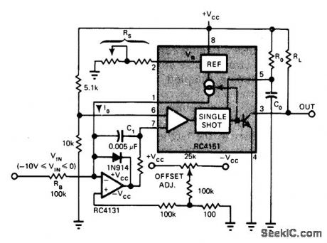
Although basedon Raytheon 4151 IC voltage-to-frequency converter,circuit is readily adapted to other modern V/F converters now costing under $10 each With values shown, input of to-10 VDC provides proportional frequency change from0 to 10 kHz at output. Design equations are given. Article also covers F/V operation of same IC for demodulating FSK data.—T. Gate, IC V/F Converters Readily Handle Other Functions Such as F/V, A/D, EDN Magazine, Jan. 5, 1977, p 82-86. (View)
View full Circuit Diagram | Comments | Reading(759)
CURE_FOR_NOISY_CONTROL
Published:2009/7/2 3:14:00 Author:May
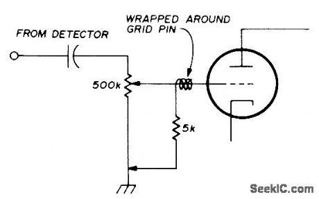
Connecting 5K resistor between grid of first AF stage and ground as shown substantially reduces noise generated by worn volume-control pot in older tube-type communication receiver. Modification can be made from top of chassis by wrapping piece of wire around grid pin of audio tube, bringing wire up alongside tube and out through top of shield. then soldering 5K resistor between wire and chassis.-J. Schroeder,Temporary Fix for Noisy Volume Controls. Ham Radio. Aug. 1974. p 62. (View)
View full Circuit Diagram | Comments | Reading(454)
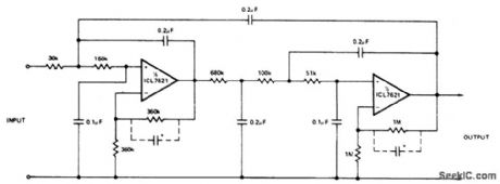
BANDPASS_FILTER
Published:2009/7/2 3:14:00 Author:May


The input signal is applied through R3 to the inverting input of the summing amplifier and the output is taken from the first integrator. The summing amplifier will maintain equal voltage at the inverting and non-inverting inputs. Defining 1/R1C1 as ω1 and 1/R2C2 as ω2, this is now a convenient form to look at the center-frequency ω0 and ftlter Q.The frequency response for various values of Q is shown. (View)
View full Circuit Diagram | Comments | Reading(0)
ACTIVE_BANDPASS_FILTER_f0_1000_Hz
Published:2009/7/2 3:10:00 Author:May

This filter has a bandpass centered around 1kHz, for applications such as bridge amplifiers, null detectors, etc.The circuit uses a μA741 IC and standard 5% tolerance components. (View)
View full Circuit Diagram | Comments | Reading(1374)
PINK_NOISE_FILTER
Published:2009/7/2 3:10:00 Author:May

Used in acoustics for measuring transducer characteristics, absorption-reflection and transmission coefficients of materials, and room parameters such as reverberation time. Offsets falloff of detected noise signal at low frequencies by using filter shown to convert random-noise source from constant energy per hertz (white-noise frequency spectrum) to constant energy per octave (pink-noise response). Filter covers audio range from 10 Hz to 20 kHz, providing -20 dB per decade transmission characteristics with three 741 opamp stages. Frequency characteristic is independent of source and load impedances. Supply voltages can be from ±6 to ±18 V.-R. Mauro, Simple Pink Noise Filter. Audio. March 1977. p 36 and 38. (View)
View full Circuit Diagram | Comments | Reading(1217)
PROGRAMMABLE_BANDPASS_USING_TWIN_T_BRIDGE
Published:2009/7/2 3:08:00 Author:May
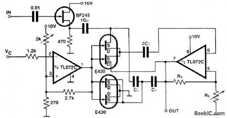
The circuit gives a programmable bandpass where both the cut-over frequency andthe gain,A,are controlled independently.In the twin-T bridge the resistors R and R/2 are replaced by two double FETs,E 430,the channel resistance of the first one in thesenes,the channel resistances of the second one are in parallel as to stimulate the resis-tance R/2. Both these resistors are controlled by Vc which ranges from 0 V to about1 V. The gain of the circuit is set by means of the resistors R2 and R3. (View)
View full Circuit Diagram | Comments | Reading(724)
RADAR_MOVING_TARGET_SIMULATOR
Published:2009/7/24 2:29:00 Author:Jessie
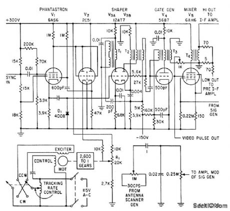
Supplies signal having all characteristics of radar echo, for testing automatic tracking radars under normal and extreme conditions. Phantastron, dual-diode V2, and two-qhase motor serve as variable time-delay.-K. L. Chapman, Moving-Target Simulator Tests Tracking Radars, Electronics, 34:13, p 58-60. (View)
View full Circuit Diagram | Comments | Reading(618)
10_MEGABIT_LINK
Published:2009/7/2 3:08:00 Author:May
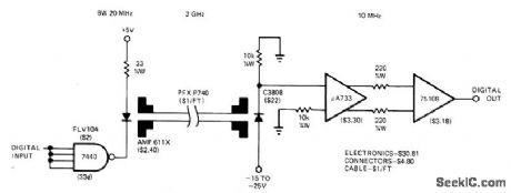
Transmitter and receiver for fiber-optiC data link between teleprinter and microDrocessor utilize wide bandwidth of cable for transmitting data at 10-megabit rate. Receiver input requires C3808 PIN photodiode.-O.E. Marvel and J. C. Freeborn. A Little HandsOn Experience llluminates Fiber-Optic Links,EDN magazine Nov,5,1977,p 71-75. (View)
View full Circuit Diagram | Comments | Reading(1657)
THYRISTOR_SPARK_QUENCHER
Published:2009/7/2 3:02:00 Author:May
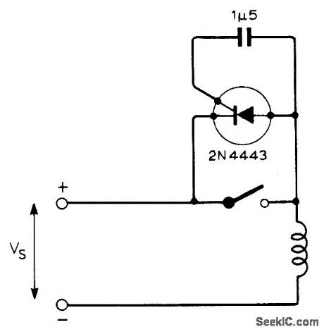
Suppresses arcing at contacts when switching large inductive loads. Use SCR capable of operating at well over twice supply voltage and passing full load current during swhch-off. SCR shown will handle up to 500 V at up to BO A provided current pulses are under 8 ms.-E. Potter. Switch Spark Quench for Inductive Loads. Wireless World. Dec. 1973. p 605. (View)
View full Circuit Diagram | Comments | Reading(735)
PRECISION,FAST_SETTLING,LOW_PASS_FILTER
Published:2009/7/2 3:02:00 Author:May

This circuit is useful where fast signal acquisition and high precision are required, as in electronic scales. The filter's time constant is set by the 2 K ohm resistor and the 1 μF capacitor until comparator No, 1 switches. The time constant is then set by the 1.5 M ohm resistor and the 1 μF capacitor. Comparator No. 2 provides a quick reset.The circuit settles to a final value three times as fast as a simple 1.5 M ohm-1μF filter, with almost no dc error. (View)
View full Circuit Diagram | Comments | Reading(679)
RADAR_TARGET_ACCELERATION_SIMULATOR
Published:2009/7/24 2:40:00 Author:Jessie
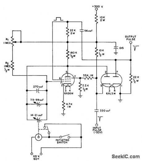
Used for testing radar range tracking systems. Uses phantastron delay modified by adding synchronous. motor. driven capacitor in feedback loop to provide target with con trolled acceleration. Pulse used to trigger phantastron corresponds to radar transmitted pulse; second pulse, triggered by trailing edge of phantastron square-wave, represents radar echo. Time between pulses, representing range, can be set to desired values by changing resistance between positive supply and grid and changing capacitance between plate and grid of phantastron tube.-Radar Target Acceleration Simulator, Electronic Circuit Design Handbook, Mactier Pub. Corp., N.Y., 1965, p 171. (View)
View full Circuit Diagram | Comments | Reading(1243)
STATE_VARIABLE_FILTER
Published:2009/7/2 2:22:00 Author:May
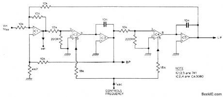
The filter produces three outputs: high-pass, bandpass, and low-pass. Frequency is linearly proportional to the gain of the two integrators. Two CA3080's, (IC2, 4) provide the variable gain, the resonant frequency being proportional to the current IABC. Using 741 op amps for IC3 a control range of 100 to 1, (resonant frequency) can be obtained.If CA3140's are used instead of 741's then this range can be extended to nearly 10,000 to 1. (View)
View full Circuit Diagram | Comments | Reading(1415)
CORE_DRIVER
Published:2009/7/24 2:36:00 Author:Jessie
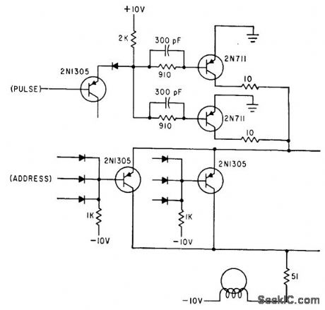
Causes current with fast rise and fall time to flow through steering driver that has been actuated by outputs of address counter used in generating programmed digital signals for simulation or test purposes.-W. D. Woo, Novel Digital Signal Generator Uses Magnetic, Core Pegboard, Electronics, 35:27, p 46-49. (View)
View full Circuit Diagram | Comments | Reading(545)
POWER_SWITCHING_CIRCUIT
Published:2009/7/2 3:00:00 Author:May
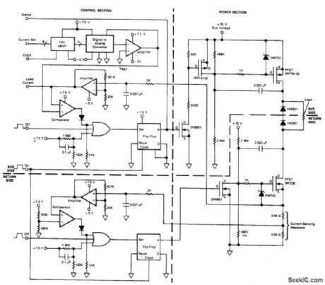
Circuit Notes
This circuit provides on/off switching, soft starting, current monitoring, current tripping, and protection against overcurrent for a 30 Vdc power supply at normal load currents up to 2 A. The switch is turned on by an“on”command pulse; it is turned off by an“off”command pulse. An overcurrent trip can also be set on the bus side by a 6-digit binary signal, which is converted to an analog voltage and compared with the amplified voltage developed across a loadcurrent-sensing resistor. Resistor/capacitor combinations(0.027 μF, 2 kO)at the inputs of the current-sensing amplifiers act as low-pass filters: this introduces a few hundred its of delay in the response to overcurrent, thereby providing some inununity to noise. The 0.022 pF capacitors connected to the drain terminals of the PFETs provide a Miller effect, which reduces the rate of change of the drain voltage and therefore the rate of rise of current at turn-on. The soft-turn-on time depends upon the load impedance and is typically 100 to 200 ms. (View)
View full Circuit Diagram | Comments | Reading(554)
NUCLEAR_BLAST_SIMULATOR
Published:2009/7/24 2:35:00 Author:Jessie
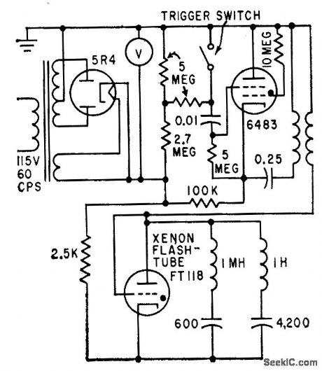
Uses xenon flashtube in double-discharge circuit to simulate thermal radiation pulse of nuclear explosion within atmosphere, which rises rapidly to first maximum, declines to minimum, rises to second maximum, then decreases gradually to zero. Used to evaluate atomic bomb alarm systems.-D. J. Baker and D. E. Thomas, Nuclear Thermal Pulse Simulator, Electronics, 32:44, p 66-69. (View)
View full Circuit Diagram | Comments | Reading(1447)
FIFTH_ORDER_CHEBYSHEV_MULTIPLE_FEEDBACK_LOW_PASS_FILTER
Published:2009/7/2 2:59:00 Author:May
The low bias currents permit high resistance and low capacitance values to be used to achieve low frequency cutoff. fc=10 Hz, Avct =4, Passband ripple = 0.1 dB.Note that small capacitors (25-50 pF) may be needed for stability in some cases. (View)
View full Circuit Diagram | Comments | Reading(483)
LASER_DIODE_SOURCE
Published:2009/7/2 2:57:00 Author:May
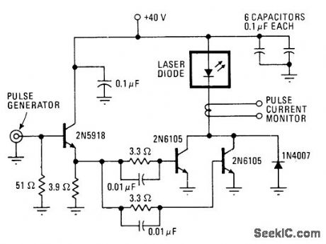
With transistor switching circuit shown for RCA SG2007 laser diode, pulses as short as 10 ns are possible at repetition rates above 100 kHz. Used in optical communication system in which fiber bundle or singlefiber is attached directly to laser pellet.-J. T. O'Brien, Laser Diodes Provide High Power for High-Speed Cornmunieations Systems, Electronics, Aug. 5, 1976, p 94-96. (View)
View full Circuit Diagram | Comments | Reading(1340)
| Pages:293/471 At 20281282283284285286287288289290291292293294295296297298299300Under 20 |
Circuit Categories
power supply circuit
Amplifier Circuit
Basic Circuit
LED and Light Circuit
Sensor Circuit
Signal Processing
Electrical Equipment Circuit
Control Circuit
Remote Control Circuit
A/D-D/A Converter Circuit
Audio Circuit
Measuring and Test Circuit
Communication Circuit
Computer-Related Circuit
555 Circuit
Automotive Circuit
Repairing Circuit