
Amplifier Circuit
Index 117
Basic_unity_gain_voltage_follower
Published:2009/7/23 21:48:00 Author:Jessie

This circuit uses one-half of a 747 connected in the classic unity-gain voltage-follower configuration, where the input impedance is high and the output impedanceis low. (View)
View full Circuit Diagram | Comments | Reading(671)
RAMP_GENERATOR_COMPARATOR
Published:2009/7/6 2:29:00 Author:May
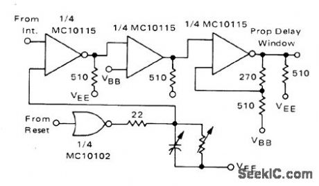
Developed for frequency counter using standard ECL components. One input to comparator is from integrator stage, and other is from ramp generator driven by reset signal from UJT oscillator.-W. R. Blood, Jr., Measure Frequency and Propagation Delay with High Speed MECL Circuit , Motorola, Phoenix, AZ, 1972, AN-586 p 3. (View)
View full Circuit Diagram | Comments | Reading(755)
READ_HEAD_PREAMPLIFIER
Published:2009/7/6 2:24:00 Author:May
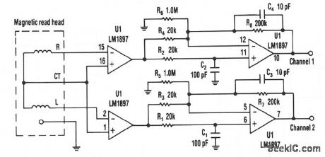
Choosing dc rather than ac coupling can reduce much of the noise associated with preamplifiers for a magnetic reading head, particularly in the low frequencies. The LM1897 eliminates the need for the capacitor that usually ac couples the read head to the preamplifier input. The read head itself has a small resistance, typically 50Ω, and so is less prone to noise pickup. Moreover, the LM1897 has a low-bias current; merely 2 μA as a worst case. Such a low-bias current flowing through the head's low resistance generates very little noise. Accordingly, even with a gain of 25, the first stage of the preamplifier circuit produces little noise. (View)
View full Circuit Diagram | Comments | Reading(853)
10_MC_SCHMITT
Published:2009/7/23 21:15:00 Author:Jessie

Will operate as square wave generator in range of 100 cps to 10 Mc, using 2N695, 2N705, or 2N711 mesa transistors.-P. A. Mclnnis, Low-Cost Computer Circuits, Motorola Application Note AN-130, Nov. 1965. (View)
View full Circuit Diagram | Comments | Reading(638)
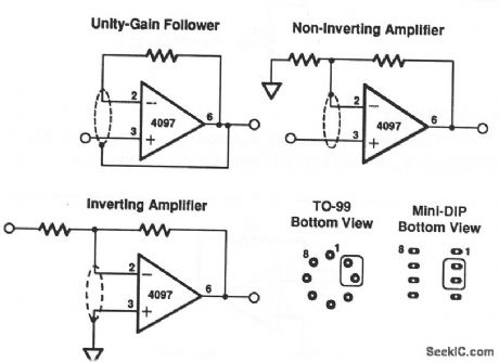
Large_signal_voltage_follower_with_000065_worst_case_accuracy_error
Published:2009/7/23 21:15:00 Author:Jessie
The input offset voltage and drift with temperature of the RC4097 that are shown in this voltage-follower circuit are trimmed at wafer test to a low level. However, if further adjustment of VOS is necessary, nulling with the circuit of Fig. 10-17B will not degrade drift with temperature. The Fig. 10-17B offset circuit has an approximate range of about 4 mV. (View)
View full Circuit Diagram | Comments | Reading(834)
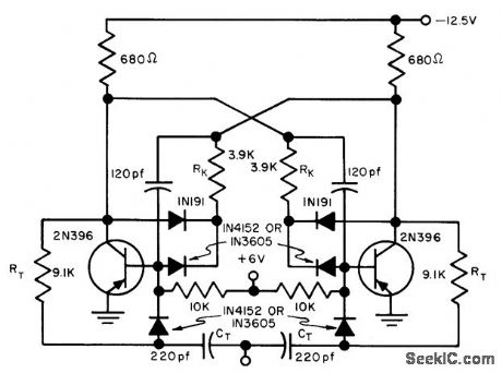
SIMPLIFIED_FULL_WAVE_UJT_SCR_TRIGGER
Published:2009/7/23 21:14:00 Author:Jessie

Consists of two basic half-wave circuits plated back to back, with emitters of ujt's cross-coupled with network that exerts full-cycle phase control over both scr's.- Transistor Manual, Seventh Edition, General Electric Co., 1964, p 330. (View)
View full Circuit Diagram | Comments | Reading(1829)
Low_duty_cycle_log_amplifier
Published:2009/7/23 21:13:00 Author:Jessie

This circuit is designed for cases where very accurate offset adjustments must be made. Coarse adjustment is provided by the offset pot at pins 9/10.The output of the 2920 is returned to the input (at pin 7), an LF356H op amp to provide soft offset correction automatically. This circuit is recommended when processing bipolar or low duty-cycle pulse signals. Rin, should match the source impedance. C2 is typically between 10 and 50 pF. (View)
View full Circuit Diagram | Comments | Reading(594)
Precision_absolute_value_amplifier_with_low_TO_TC_VSUBOS_SUB
Published:2009/7/23 21:13:00 Author:Jessie
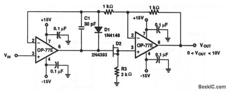
The high gain and low temperature-coefficient output offset voltage of the OP-77E assures accurate operation with inputs from microvolts to volts. In this circuit, the signal always appears as a common-mode signal to the op amps. The OP-77E CMRR of 1 μV/V assures errors of loss than 2 ppm. (View)
View full Circuit Diagram | Comments | Reading(883)
Transformerless_microphone_preamplifier
Published:2009/7/23 21:12:00 Author:Jessie
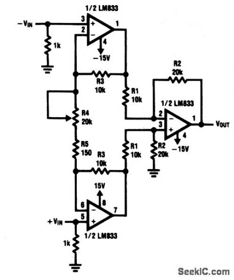
This circuit uses two LM833s to amplify the input signal before the common-mode noise is cancelled in the differential amplifier. The equivalent input noise is about 760 nV over a 20-Hz to 20-kHz frequency band (-122 dB referred to 1V), which is over 26 dB lower than a typical microphone output from the 30-dB SPL ambient noise level in a quiet room. THD is under 0.01% at maximum gain, and 0.002% at minimum gain. R4 adjusts the circuit gain from about 4 to 270.Common-mode noise is about 60 dB (or 44 dB, worst case) when R1, R2, and R3 are of 0.1 % tolerance. If better common-mode rejection is needed, one or the R2s can be replaced with an 18-kΩ resistor and a 5-kΩ, pot to trim for a better CMRR.If necessary, use 470-pF capacitors between inputs and ground to prevent RF interference from entering the preamp inputs. (View)
View full Circuit Diagram | Comments | Reading(899)
THREE_INPUT_TRIGGER
Published:2009/7/23 21:11:00 Author:Jessie
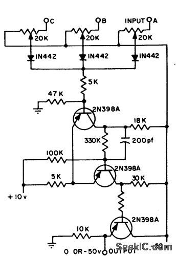
Digital logic permits use of only one Schmitt trigger for monitoring number of variables that can have different voltage levels at which trigger action is desired. Potentiometers provide independent control of set points for each positive input. Each input then triggers circuit independently at its particular theshold, pro vided circuit was not previously triggered. Circuit is taken from NASA-SP-5022 Technology Utilization Report, Lewis Research Center.-Multiple-Input Trigger Circuit, Electromechanical Design, Nov. 1965, p 66. (View)
View full Circuit Diagram | Comments | Reading(528)
BASE_TRIGGERING_WITH_HYBRID_GATE
Published:2009/7/23 21:18:00 Author:Jessie
Combines sensitivity of base triggering and trigger amplitude variation of collector triggering. Bias potential varies in order to direct trigger pulse more effectively. This steering scheme is attractive for some nonsaturated circuits, when collector-base voltage for conducting transistor is very small- Transistor Manual, Seventh Edition, General Electric Co., 1964, p 199. (View)
View full Circuit Diagram | Comments | Reading(624)
Resistor_multiplier
Published:2009/7/23 21:17:00 Author:Jessie
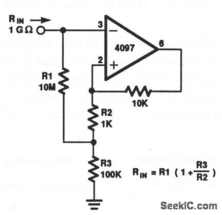
This circuit appears as a high resistance to the input. The resistance value depends on R1, R2, and R3 (1 GΩ using the values shown). (View)
View full Circuit Diagram | Comments | Reading(0)
1_MC_SCHMITT_TRIGGER
Published:2009/7/23 21:16:00 Author:Jessie

Q1 conducts when input exceeds 6.8 v. Q2 always conducts if input is below 5.2 v. Ambient temperature range is 0 to 71℃. Output at collector has 2 v minimum level change.- Transistor Manual, Seventh Edition, Geneml Electric Co., 1964, p 200. (View)
View full Circuit Diagram | Comments | Reading(669)
Typical_guard_ring_layout_for_op_amps
Published:2009/7/23 21:16:00 Author:Jessie
Even with properly cleaned and coated PC boards, leakage currents can limit the circuit performancc under severe environmental conditions. These currents can be intercepted before they reach the op-amp inputs by a guard ring or a conductor in the leakage path. The ring should surround the input terminals, and should be at the same potential as the inputs. Notice that the guard ring for the inverting and noninverting configurations connects to the inputs, while the unity-gain circuit connects to the output. (View)
View full Circuit Diagram | Comments | Reading(2406)
Basic_noninverting_amplifier
Published:2009/7/23 21:35:00 Author:Jessie

This circuit shows an LM107 that is connected in the classic noninverting amplifier configuration, where VOUT follows VIN The amplitude of the output depends on the ratio of R1 and R2 (within the limits of the supply voltage). The parallel resistance of R1 and R2 should equal the source resistance. (View)
View full Circuit Diagram | Comments | Reading(466)
Low_noise_low_power_amplifier
Published:2009/7/23 21:34:00 Author:Jessie

This circuit shows an SL560 used as a low-noise, low-power consumption amplifier. (View)
View full Circuit Diagram | Comments | Reading(517)
Composite_high_speed_precision_amplifier
Published:2009/7/23 21:21:00 Author:Jessie

This circuit provides a gain of 10 with the values shown. (View)
View full Circuit Diagram | Comments | Reading(667)
TRANSIENT_REJECTING_SCR_TRIGGER
Published:2009/7/23 21:21:00 Author:Jessie
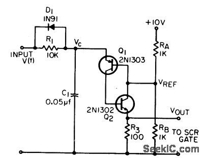
Integrator combined with voltage comparator detects difference in voltage-time areas of data pulses and random transients. Dotc pulses passed are 8 v high and 0.5 millisec wide.-S. B. Marshall, Noise-Rejecting SCR Trigger Circuit, EEE, 14:7, p 102-104. (View)
View full Circuit Diagram | Comments | Reading(620)
Low_phase_shift_IF_limiter
Published:2009/7/23 21:26:00 Author:Jessie
The SL532 shown here is used for wide-bandwidth limiting IF strips.With the values shown, the input signal for full limiting is 300 μV (rms)(-57 dBm), the output is limited to 1 Vpp, with a phase shift of ±3%. (View)
View full Circuit Diagram | Comments | Reading(602)
Battery_manager
Published:2009/7/23 21:25:00 Author:Jessie
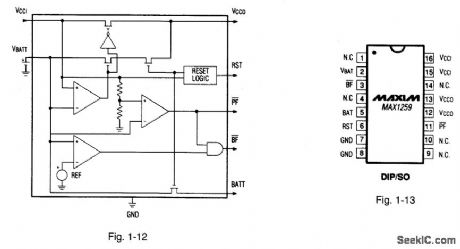
Figures 1-12 and 1-13 show the block diagram and pin configuration; respectively, for the MAX1259. The IC is similar to that described for Fig. 1-N, and switches to the backup battery when the primary power supply is interrupted. The input-output differential is 200 mV when supplying 250mA from the primary power or 15mA from the battery. The battery-failure output at pin 3 indicates when the battery is below +2 V. The power-fail output at pin 11 indicates when the primary power is low. MAXIM NEW RELEASES DATA BOOK, 1992, P. 5-17. (View)
View full Circuit Diagram | Comments | Reading(631)
| Pages:117/250 At 20101102103104105106107108109110111112113114115116117118119120Under 20 |
Circuit Categories
power supply circuit
Amplifier Circuit
Basic Circuit
LED and Light Circuit
Sensor Circuit
Signal Processing
Electrical Equipment Circuit
Control Circuit
Remote Control Circuit
A/D-D/A Converter Circuit
Audio Circuit
Measuring and Test Circuit
Communication Circuit
Computer-Related Circuit
555 Circuit
Automotive Circuit
Repairing Circuit