
Amplifier Circuit
Index 116
Stabilized_ultra_wideband_current_mode_feedback_amplifier
Published:2009/7/23 20:32:00 Author:Jessie
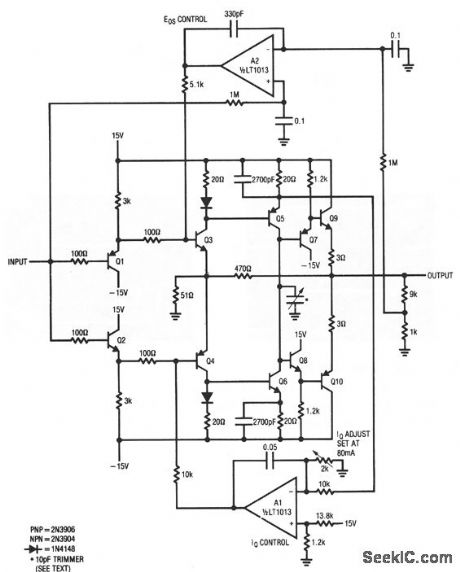
virtually any video or wideband application. For gains from 1 to 20, full-power bandwidth is 25 MHz, with the -3-dB point beyond 110 MHz. Gain is sot for 10 (with the values shown) by the 51- and 470-Ω Q3/Q4 emitter resistors. Slew rate exceeds 3000 V/μs.Damping is optimized with the 10-pF trimmer at the Q5/Q6 collectors. To use the circuit, adjust the IQ level to 80 mA immediately after turn on. Next, sot the A2 input resistor divider to a ratio appropriate to the closed-loop gain (1 and 9 kΩ, in this case). Finally, adjust the 10-pF trimmer for best results (preferably with a square-wave input). Notice that this circuit has no output protection. (View)
View full Circuit Diagram | Comments | Reading(951)
Fast_precision_inverter_with_100_V_μs_slew_rate
Published:2009/7/23 20:28:00 Author:Jessie
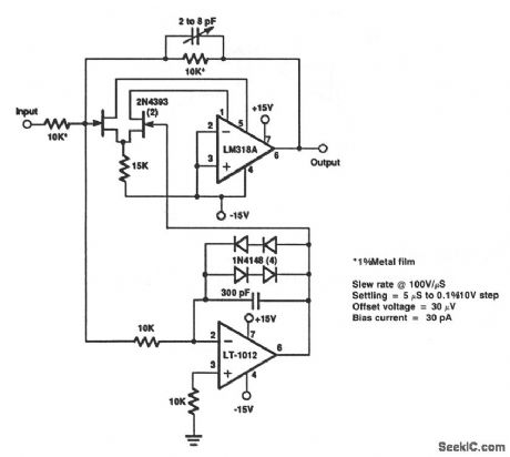
This circuit has a setting time of 5μs to 0.1% with a 10-V step input. (View)
View full Circuit Diagram | Comments | Reading(869)
Log_amplifier
Published:2009/7/23 20:24:00 Author:Jessie

Compare this op-amp circuit to the log-amplifier circuits of chapters 2 and 3.
(View)
View full Circuit Diagram | Comments | Reading(0)
Precision_current_sink
Published:2009/7/23 20:22:00 Author:Jessie
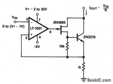
As shown, the ability of this circuit to sink current depends on VIN and the value of R. Note that VIN can be anything from 0 to (V + - 1 V), and V+ can be +2 to +35 V. (View)
View full Circuit Diagram | Comments | Reading(1)
ZERO_HYSTERESIS_SCHMITT
Published:2009/7/23 20:46:00 Author:Jessie

Turn-on and turn-off voltages are made identical by using zener diode in place of RE.-R. A. Wilson, Zero-Hysteresis Schmitt Trigger, EEE, 13:2, p 62. (View)
View full Circuit Diagram | Comments | Reading(669)
EMITTER_TRIGGERED_FLIP_FLOP
Published:2009/7/23 20:45:00 Author:Jessie
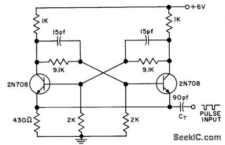
Pulse input, makes alternate sides of flip-flop conduct on alternate trigger pulses. Maximum trigger rate exceeds 2 Mc with trigger amplitude from 4 to 12 v. Chief limitation is high trigger current required.- Transistor Manual, Seventh Edition, General Electric Co., 1964, p 196. (View)
View full Circuit Diagram | Comments | Reading(678)
Single_op_amp_difference_amplifier
Published:2009/7/23 20:39:00 Author:Jessie

This circuit provides a voltage gain of 1000 for difference-signal inputs. For example, if the inverting input is 10 μV and the noninverting input is 11 μV, the difference is 1 μV and the output is 1000 μV. Figure 10-14B shows an offset nulling circuit (if required). (View)
View full Circuit Diagram | Comments | Reading(778)
Mini_power_amplifier
Published:2009/7/23 20:37:00 Author:Jessie
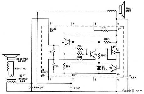
This little LM3909 audio amplifier can be operated as a one-way intercom or for listening in on various situations. Operating current is only 12 to 15 mA. The circuit can hear fairly faint sounds, and someone speaking directly into the microphone generates a full 1.4-V peak-to-peak at the speaker. (View)
View full Circuit Diagram | Comments | Reading(737)
FOUR_CHANNEL_D_A_OUTPUT_AMPLIFIER
Published:2009/7/6 3:14:00 Author:May

View full Circuit Diagram | Comments | Reading(536)
Inverting_amplifier_for_gains_less_than_10
Published:2009/7/23 21:06:00 Author:Jessie
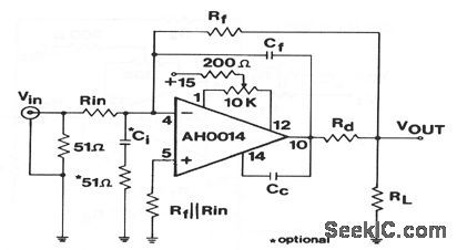
This circuit shows an AH0014 connected as an inverting wideband amplifier, where gain must be less than 10, but more than 1. The characteristics are the same as for the circuit of Fig. 3-49, but layout is more critical. Keep all leads as short as possible. Solder chip capacitors (bypass capacitors) directly to the chip pins. Use a ground plane. For best results, use an Ri of 1 kΩ or less, and keep Ci in the 15- to 60-pF range (use a variable Ci and adjust for best results. Figure 3-48B shows external connections for the AH0014. (View)
View full Circuit Diagram | Comments | Reading(614)
FAST_RECOVERY_COLLECTOR_TRIGGERING
Published:2009/7/23 21:06:00 Author:Jessie
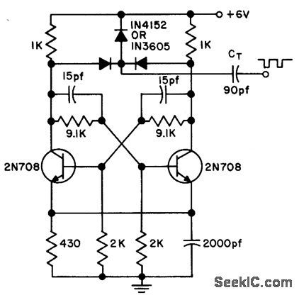
Additional diode, used in place of resistor from midpoint of diode pair to +6 v, has high back impedance to prevent shunting of trigger pulse during triggering period, and has low forward impedance to insure fast recovery. - Transistor Manual, Seventh Edition, General Electric Co., 1964, p 198. (View)
View full Circuit Diagram | Comments | Reading(577)
Inverting_amplifier_for_gains_greater_than_10
Published:2009/7/23 21:04:00 Author:Jessie

This circuit shows an AH0014 connected as an inverting wideband amplifier, where gain must be greater than 10. If the gain is over 100, Cc can generally be omitted. For best results, use an Rf of 1 kΩ or less (to minimize the effects of stray capacitance). When Cc is in the 10-pF range, a stable gain of 20 dB is possible at 10 MHz. If peaking occurs, tower Cc to the 1- to 5-pF range. Atypical value for CF (when used) is 1 to 5 pF. A typical value for Rd (when used) is 33Ω.Figure 3-48B shows external connections for the AH0014. (View)
View full Circuit Diagram | Comments | Reading(663)
Composite_amplifier_with_current_boost
Published:2009/7/23 21:03:00 Author:Jessie

In this circuit, A1 is used to improve the dc characteristics of A2, which, in turn, determines the bandwidth of A3. Using an OP-07 for A1, an AH0014 for A2, and an AH0010 for A3, the circuit is capable of driving a 51-Ω load at±5 V to 10 MHz. Drift is less than 1μV/℃ with an offset of 20 μV. Figure 3-48B shows the external connections for the AH0014. (View)
View full Circuit Diagram | Comments | Reading(590)
High_speed_fast_settling_pulse_amplifier
Published:2009/7/23 21:01:00 Author:Jessie

In this circuit, the amplifier is set for unity gain. The input signal is terminated into 51Ω. This resistance, together with the 470-pF capacitor, compensates for stray capacitances that might appear at the input. With the values shown (and the variable capacitor adjusted to 5 pF), the output is± 10 V swing at ±50-mA drive current, with unity gain up to 100 MHz (assuming a typical ± 15-V supply. The pin connections are: 1 output, 10 +Vcc, 11-Vcc, 16-input, 19 +input, 20 common. (View)
View full Circuit Diagram | Comments | Reading(814)
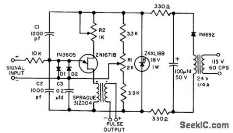
TRANSIENT_ATTENUATING_TRIGGER
Published:2009/7/23 21:01:00 Author:Jessie
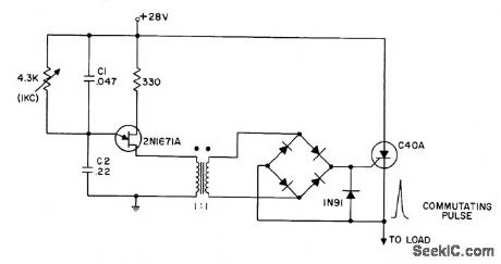
Transformer coupling and diode bridge between ujt and scr greatly attenuate transients, to prevent premature triggering of ujt when used for impulse commutation in d-c choppers and invertors.- Transistor Manual, Seventh Edition, General Electric Co., 1964, p 333. (View)
View full Circuit Diagram | Comments | Reading(562)
CURRENT_SENSING
Published:2009/7/23 20:50:00 Author:Jessie
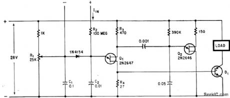
Input current of only 40 no will charge C2 and raise voltage at emitter of Q1 to triggering level. C1 and C2 then discharge through R4, und resulting generating pulse triggers scr D1 in series with load. Recovery is rapid.-D. V. Jones, Quick-On-The-Trigger Design, Electronics, 38:12, p 105-110. (View)
View full Circuit Diagram | Comments | Reading(1405)
UJT_TRIAC_PHASE_CONTROL
Published:2009/7/23 21:00:00 Author:Jessie
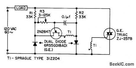
Has wide range of stable control, without hysteresis or dependence upon supply voltage. Used in automatic feedback control systems, since ujt is essentially half of balanced bridge, with bulb-in unbalance detection.- Transistor Manual, Seventh Edition, General Electric Co., 1964, p 330. (View)
View full Circuit Diagram | Comments | Reading(969)
VOLTAGE_SENSING_TRIGGER
Published:2009/7/23 20:55:00 Author:Jessie
Long-term stability is better than 10 mv, and can be improved still more by adding two silicon diodes in series with R2. Ideal for use in go-no-go applications.- Transistor Manual, Seventh Edition, General Electric Co., 1964, p 325. (View)
View full Circuit Diagram | Comments | Reading(647)
LOW_LEVEL_THRESHOLD_DETECTOR
Published:2009/7/23 20:51:00 Author:Jessie

Determines when millivolt-range signal exceeds adjustable threshold. Circuit is similar to Schmitt trigger. Forward gain of amplifier is increased by adding second differential amplifier stage having two low-cost transistors and three resistors. Hysteresis can be as low as 2 mv, as compared to 100 mv in standard Schmitt.-R. M. Muth, Stable Threshold Circuit With Low Hysteresis, EEE, 14:1, p 64. (View)
View full Circuit Diagram | Comments | Reading(930)
Differentiator
Published:2009/7/23 21:52:00 Author:Jessie
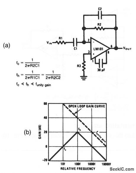
This circuit was originally developed to perform the mathematical operation of differentiation in analog computers. As shown by the frequency-response plot of Fig. 10-40B, a differentiator is actually a form of filter. R2/C2 form a 6-dB per octave rolloff network in the feedback, and R1/C1 form a similar network at the input. (View)
View full Circuit Diagram | Comments | Reading(1479)
| Pages:116/250 At 20101102103104105106107108109110111112113114115116117118119120Under 20 |
Circuit Categories
power supply circuit
Amplifier Circuit
Basic Circuit
LED and Light Circuit
Sensor Circuit
Signal Processing
Electrical Equipment Circuit
Control Circuit
Remote Control Circuit
A/D-D/A Converter Circuit
Audio Circuit
Measuring and Test Circuit
Communication Circuit
Computer-Related Circuit
555 Circuit
Automotive Circuit
Repairing Circuit