
Amplifier Circuit
Index 108
30_MC_VARIABLE_BANDWIDTH_RADAR_PREAMP
Published:2009/7/21 6:17:00 Author:Jessie
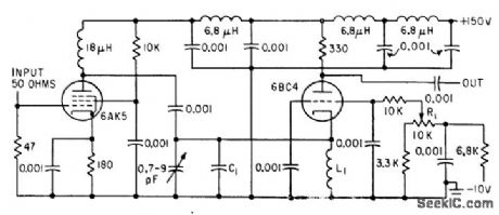
Bias control R1 on grounded-grid 6BC4 triode provides continuous change of bandwidth from 200 kc to 15 Mc, for changing search range. Insertion loss is 0 db.-R. Hirsch, Voltage-Variable Bandwidth Filter, Electronics, 35:22, p 46-47. (View)
View full Circuit Diagram | Comments | Reading(848)
L_F_D_F_PREAMP
Published:2009/7/21 6:15:00 Author:Jessie
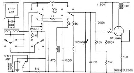
Negative feedback provides stability, yet gain is sufficient so noise contributions of preamplifier to 15-500 kc direction-finding receiver are negligible. Output of preamp feeds receiver through 100 feet of 100-ohm balanced transmission line.-L. E. Orsak and D. W. Martin, Direction Finding at Low Frequencies, Electronics, 33:38, p 74-77. (View)
View full Circuit Diagram | Comments | Reading(509)
ELECTROMETER_PREAMP
Published:2009/7/21 6:13:00 Author:Jessie
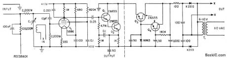
Transformer T1 feeds drive coil of vibrating capacitor C1 used in place of conventional chopper for measuring picoampere currents. Output of electrometer, taken from Q2 of preamp, goes to amplifier that is source of feedback signal. -V. J. Caldecourt, Using a Vibrating Capacitor as an Electrometer Input, Electronics, 35:14, p 48-50. (View)
View full Circuit Diagram | Comments | Reading(1184)
35_4_MHz_TUNABLE_IF_WITH_NOISE_BLANKING
Published:2009/7/7 23:47:00 Author:May


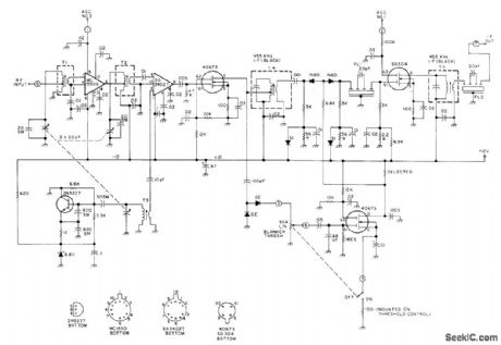
MC1550G is followed by Silicon General 563402T mixer that provides good conversion gain with very light oscillator loading. Mixer output is fed to 40673 amplifier that builds up noise spikes for blanker consisting of 1N60 diode gate and 40673 pulse amplifier. Blanker is fed from envelope detector that controls gate feeding FL1 dual ceramic filter providing IF selectivity. IF stage following blanker uses SD304 dual-gate MOSFET, transformer-coupled to ceramic filter FL2 at IF output. Article gives construction details.-R. Megirian, The Minicom Receiver, 73 Magazine, April 1977, p 136-149. (View)
View full Circuit Diagram | Comments | Reading(1515)
DIRECT_COUPLED_PREAMPLIFIER
Published:2009/7/21 6:31:00 Author:Jessie
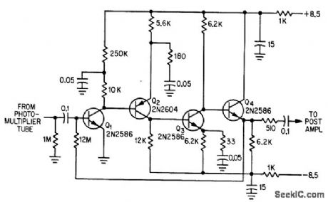
Output of multiplier phototube in orbiting astronomical observatory receives closed-loop amplification of 12 in current-sensing preamplifier over input dynamic current range of 3 to 500 ma. -R. Cuikay and T. Callahan, Orbiting Observatory to Measure Stars' Dim Light, Electronics, 37:9, p 28-31. (View)
View full Circuit Diagram | Comments | Reading(689)
AUTOPILOT_PREAMP
Published:2009/7/21 6:29:00 Author:Jessie

Reliable pitch-axis channel uses four npn silicon transistors.-C. W. McWilliams, Designing Safety Into Automatic Pilot Systems, Electronics, 31:45, p 69-71. (View)
View full Circuit Diagram | Comments | Reading(511)
6217_PHOTOMULTIPLIER_PREAMP
Published:2009/7/21 6:27:00 Author:Jessie

Used between photomultiplier and dual-beam oscilloscope to amplify signal pulse corresponding to transmitted laser signal in optical ranging system. Distance between transmitted and received pulses on cro corresponds to range. -M. L. Stitch, E. J. Woodbury and J. H. Morse, Optical Ranging System Uses Laser Transmitter, Electronics, 34:16, p 51-53. (View)
View full Circuit Diagram | Comments | Reading(530)
7326_PHOTOMULTIPLIER_PREAMP
Published:2009/7/21 6:26:00 Author:Jessie
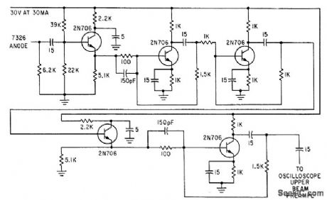
Used between type 7326 photomultiplier and dualbeam oscilloscope in receiver of optical ranging system. Voltage gain is 100 for output dynamic range of 1.5 V, but noise figure is only about 14 db.-M. L. Stitch, E. J. Woodbury and J. H. Morse, Optical Ranging System Uses Laser Transmitter, Electronics, 34:16, p 51-53. (View)
View full Circuit Diagram | Comments | Reading(624)
LOW_NOISE_TAPE_RECORDER_PREAMP
Published:2009/7/21 6:24:00 Author:Jessie
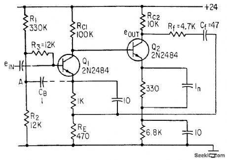
Closed-loop gain is 20 db from 100 cps to nearly 8 Mc for source impedance of 1,000 to 6,000 ohms.-J. J. Rado, Designing Input Circuits with Lowest Possible Noise, Electronics, 36:31, p 46-49. (View)
View full Circuit Diagram | Comments | Reading(842)
TELEPHONE_AMPLIFIER
Published:2009/7/7 22:53:00 Author:May
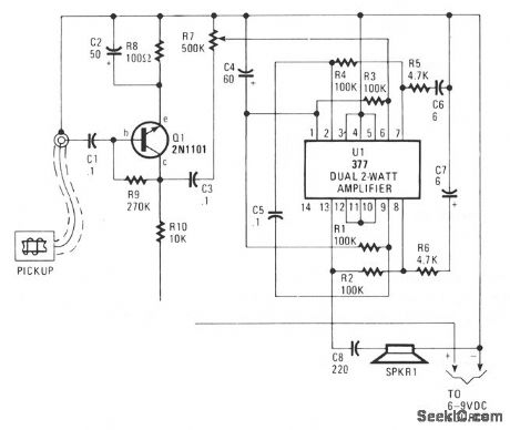
Audio from the telephone is inductively coupled to the base of Q1, which is used as a preamp. The preamp provides a gain of about 75 dB, to boost the input signal from about 4 mV to about 300 mV pk-pk. If you use a higher gain transistor, increase the value of R9 to produce a Q point, measured from minus to the collector of Q1, of one-half the supply voltage. The Q1 output signal is coupled through C3 to R7, which serves as a volume or drive-level control, to U1, a dual, 2 w amplifier connected in cascade. Pins 1 through 7 serve as a driver for the final amplifier, pins 8 through 13. Compensation and balance is accomplished by components R1 through R6 and C4, C6, and C7. Pins 3 through 5, and 10 through 12 should be tied to the negative supply rail. (View)
View full Circuit Diagram | Comments | Reading(0)
DUPLEX_LINE_AMPLIFIER
Published:2009/7/7 22:15:00 Author:May
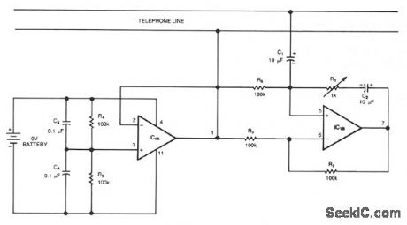
This circuit is a bidirectional amplifier that can amplify both signals of a duplex telephone conversation. It uses the principle of negative resistance. Obviously, such an amplifier could easily be unstable; however, you can adjust R1 for maximum amplification and the circuit will remain stable. The LM324 op amps can be replaced with op amps that would distort less, such as the LM1558, LF412, LF353, or LF442. (View)
View full Circuit Diagram | Comments | Reading(1049)
ASUP2_SUP_BSUP2_SUP
Published:2009/7/7 21:48:00 Author:May

Transfer function Vour = (A2-B2)/10 is easily generated by AD534 analog multiplier.Differential inputs on Z terminals permit addition of feedback attenuator to decrease scale factor (or increase signal gain) from 40 to nominal value of 10. Feedback attenuation increases output offset proportionally; to make offset adjustment, connect 4.7-megohm resistor between Z1 and wiper of 50K pot connected across power supplies.-R. Frantz, Analog Multipliers-New IC Versions Manipulate Real-World Phenomena with Ease, EDN Magazine, Sept. 5, 1977, p 125-129. (View)
View full Circuit Diagram | Comments | Reading(746)
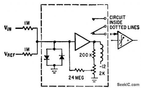
FOUR_CHANNEL_ANALOG_MULTIPLEXER
Published:2009/7/7 21:04:00 Author:May

Buffered input and output provide very high input impedance and low output impedance for analog signal selection or time-division multiplexing with Harris HA-2400/HA-2405 IC that combines functions of analog switch and high-performance opamp. Bandwidth is about 8 MHz. Signal is fed back from output to digitally selected input channel to place that channel in voltage-follower configuration with noninverting unity gain.- Linear & Data Acquisition Products, Harris Semiconductor, Melbourne, FL, Vol. 1, 1977, p 7-36-7-38 (Application Note 514). (View)
View full Circuit Diagram | Comments | Reading(2614)
SECONDARY_EMISSION_PENTODE_TRIGGER
Published:2009/7/21 9:04:00 Author:Jessie
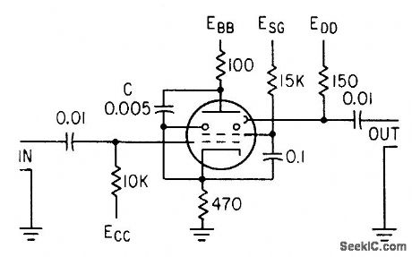
Produces positive output pulse across dynode loud each time it is triggered by positive grid pulse. Used in high-speed, short-duration pulse work.-E. J. Martin, Jr., How to Use the Secondary-Emission Pentode, Electronics, 33:41, p 60-63. (View)
View full Circuit Diagram | Comments | Reading(572)
PUSH_PUSH_OUTPUT_DOUBLER
Published:2009/7/21 7:45:00 Author:Jessie

Input is conventional push-pull configuration providing out-of-phase signals for both transistors, but for output circuit both transistors operate in parallel into standard pi network. This cancels fundamental and odd-order harmonics, leaving only second harmonic predominating in output circuit. Transistors can be 2N1692.-W. A. Rheinfelder, Choosing the Best Transmitter Output Stage, EEE, 11:10, p 48-53.
(View)
View full Circuit Diagram | Comments | Reading(992)
OPERATIONAL_TRIGGER
Published:2009/7/21 7:54:00 Author:Jessie
Combines some features of operational amplifier with those of Schmitt trigger. Input diodes prevent amplifier saturation.-P. Lefferts, Operational Trigger For Precise Control, Electronics, 37:28, p 50-55. (View)
View full Circuit Diagram | Comments | Reading(562)
LOW_POWER_INSTRUMENTATION_AMPLIFIER
Published:2009/7/7 9:12:00 Author:May
View full Circuit Diagram | Comments | Reading(0)
THERMOCOUPLE_PREAMPLIFIER
Published:2009/7/7 9:11:00 Author:May
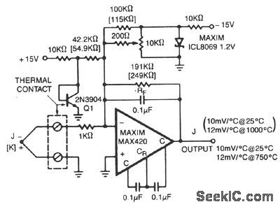
The MAX420 is operated at a gain of 191 to convert the 52 μV/'℃ output of the type J thermo-couple to a 10 mV/℃ signal. The -2.2 mV/℃ tempco of the 2N3904 is added into the summing junction with a gain of 42.2 to provide cold-junction compensation. The ICL8069 is used to remove the offset caused by the 600-mV initial voltage of the 2N3904. Adjust the 10-KΩ trimpot for the proper reading with the 2N3904 and isothermal connection block at a temperature near the center of the cir-cuit's operating range. Use the component values shown in parentheses when using a type K thermo-couple. (View)
View full Circuit Diagram | Comments | Reading(790)
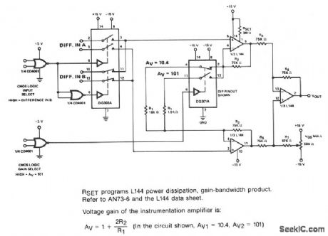
DIFFERENTIAL_INSTRUMENTATION_AMPLIFIER
Published:2009/7/7 9:09:00 Author:May
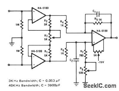
This circuit relies on extremely high input impedance for effective operation. The HA-5180 with its JFET input stage, performs well as a pre-amplifier. The standard three amplifier conftgura-tion is used with very close matching of the resistor ratios R5/R4 and (R1 + R8)/R6, to insure high common-mode rejection (CMR). The gain is con-trolled through fi3 and is equal to 2R1/R3. Additional gain can be had by increasing the ratios R5/R4 and (R7 + R8)/R6. The capacitors C1 and C2 improve the ac response by limiting the effects of transients and noise. Two suggested values are given for maximum transient suppression at fre-quencies of interest. Some of the faster DVM's are operating at peak sampling frequency of 3-kHz, hence the 4-kHz, low-pass time constant. The 40-kHz, low-pass time constant for ac voltage ranges is an arbitrary choice, but should be chosen to match the bandwidth of the other components in the sys-tem. C1 and C2 might however, reduce CMR for ac signals if not closely matched. Input impedances have also been added to provide adequate dc bias currents for the HA-5180 when open-circuited. (View)
View full Circuit Diagram | Comments | Reading(672)
BIOMEDICAL_INSTRUMENTATION_DIFFERENTIAL_AMPLIFIER
Published:2009/7/7 8:58:00 Author:May
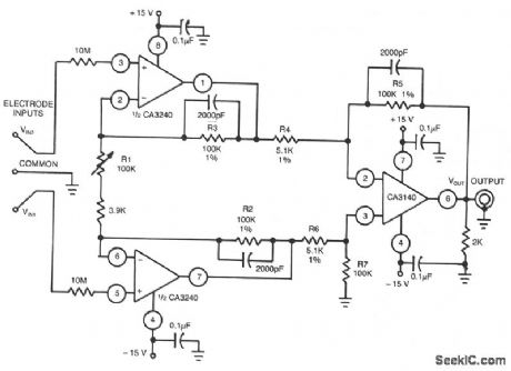
This differential amplifier uses the isolated high-impedance inputs of the CA3420 BiMOS op amp. Because the CA3240's input current is only 50 pA maximum, 10-MΩ resistors can be used in series with the input probes to limit the current to 2 μA under a fault condition. (View)
View full Circuit Diagram | Comments | Reading(1869)
| Pages:108/250 At 20101102103104105106107108109110111112113114115116117118119120Under 20 |
Circuit Categories
power supply circuit
Amplifier Circuit
Basic Circuit
LED and Light Circuit
Sensor Circuit
Signal Processing
Electrical Equipment Circuit
Control Circuit
Remote Control Circuit
A/D-D/A Converter Circuit
Audio Circuit
Measuring and Test Circuit
Communication Circuit
Computer-Related Circuit
555 Circuit
Automotive Circuit
Repairing Circuit