
Amplifier Circuit
Index 109
WIDEBAND_INSTRUMENTATION_AMPLIFIER
Published:2009/7/7 8:56:00 Author:May
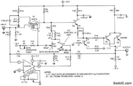
Has an input resistance of 1-MΩ, a bandwidth from dc to about 35 MHz, and a gain of 10 times. Low-frequency gain is provided by a CA3130 BiMOS op amp operated as a single-supply amplifier. High-fre-quency gain is provided by a 40673 dual-gate MOSFET. The entire amplifier is nulled by shorting the input to ground and adjusting R9 for zero dc output voltage. (View)
View full Circuit Diagram | Comments | Reading(638)
INSTRUMENTATION_AMPLFIER
Published:2009/7/7 8:55:00 Author:May
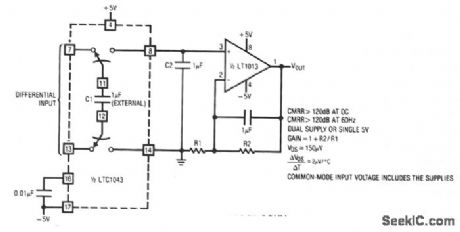
LTC1043 and LT1013 dual op amps are used to create a dual instrumentation amplifier using just two packages. A single DPDT section converts the differential input to a ground-referred single-ended signal at the LT1013's input. With the input switches closed, C1 acquires the input signal. When the input switches open, C2's switches close and C2 receives charge. Continuous clocking forces C2's voltage to equal the difference between the circuit's inputs. The 0.01-μF capacitor at pin 16 sets the switching fre-quency at 500 Hz. Common-mode voltages are rejected by over 120 dB and drift is low. (View)
View full Circuit Diagram | Comments | Reading(564)
STRAIN_GAUGE_INSTRUMENTATION_AMPLIFIER
Published:2009/7/7 8:52:00 Author:May

This circuit has an overall gain of 320. More gain can easily be obtained by lowering the value of R2. UntrimmedVOS is 10 μN, andVOS tempco is less than 0.1 μV/℃. In many circuits, the OP07 can be omit-ted, with the two MAX421 differential outputs connected directly to the differential inputs of an integrating a/d. (View)
View full Circuit Diagram | Comments | Reading(2211)
TRIGGER_WITH_TRANSMISSION_LINE_FEED_BACK
Published:2009/7/21 8:03:00 Author:Jessie

Feedback capacitor is replaced by open-circuited section of transmission line, Duration of output pulse taken across dynode load of secondary-emission penlode is adjusted by varying line length.-E. J. Martin, Jr., How to Use the Secondary-Emission Pentode, Electronics, 33:41, p 60-63. (View)
View full Circuit Diagram | Comments | Reading(523)
VOLTAGE_LEVEL_TRIGGER
Published:2009/7/21 8:00:00 Author:Jessie

Output pulse appears when input is 6.0 v but not for inputs up to 7 volts above or below this level. Circuit then continues on until input drops below 5.4 v.-R. F. Woody, Precise 6-Volt Input Triggers Circuit, Electronics, 38:14, p 80. (View)
View full Circuit Diagram | Comments | Reading(862)
RESISTOR_TESTER
Published:2009/7/21 7:59:00 Author:Jessie

Operational trigger is tripped by bridge circuits when resistor under test is 0.11% high for switch position shown. Reversing switch gives same sensitivity for low resistors.-P. Lefferts, Operational Trigger For Precise Control, Electronics, 37:28, p 50-55. (View)
View full Circuit Diagram | Comments | Reading(611)
ULTRA_PRECISION_INSTRUMENTATION_AMPLIFIER
Published:2009/7/7 8:35:00 Author:May

This circuit will run from a single 5 V power supply. The LTC1043 switched-capacitor instrumentation building block provides a differential-to-single-ended transition using a flying-capacitor technique. C1 alter-nately samples the differential input signal and charges ground referred C2 with this information. The LTC1052 measures the voltage across C2 and provides the circuit's output. Gain is set by the ratio of the amplifier's feedback resistors. Normally, the LTC1052's output stage can swing within 15 mV of ground. If operation all the way to zero is required, the circuit shown in dashed lines can be employed. This conftgu-ration uses the remaining LTC1043 section to generate a small negative voltage by inverting the diode drop. This potential drives the 10-KΩ, pull-down resistor, forcing the LTC1052's output into class A oper-ation for voltages near zero. Note that the circuit's switched-capacitor front-end forms a sampled-data filter allowing the common-mode rejection ratio to remain high, even with increasing frequency. The 0.0047μF unit sets front-end switching frequency at a few hundred Hz. (View)
View full Circuit Diagram | Comments | Reading(1113)
SCR_IMPROVES_SCHMITT_TRIGGER_STABILITY
Published:2009/7/21 8:08:00 Author:Jessie
Input signals to 200 kc give consistent triggering over wide range of temperature, source impedance, and input impedance, and hysteresis is reduced by order of 10.-M.Schmidt, Improved Schmitt Trigger Uses SCR, Electronics, 36:17, p 68. (View)
View full Circuit Diagram | Comments | Reading(702)
CUTOFF_SCHMITT
Published:2009/7/21 8:07:00 Author:Jessie
Conventional current-feedback version, In which one of the two active transistor elements is generally cut off, Per-forms reliably even though optimum operating regions for transistors cannot always be achieved.-H. Inose, Y. Yoshida, and H. Toda, Noncutoff Circuits Improve Trigger Switching, Electronics, 35:30, p 36-39. (View)
View full Circuit Diagram | Comments | Reading(603)
SCR_TRIGGER
Published:2009/7/21 8:06:00 Author:Jessie
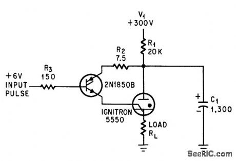
Silicon controlled rectifier triggers ignitron when 6-v pulse is applied to gate.-L. E. Frenzel, Jr., Silicon Controlled Rectifier Triggers ignition, Electronics, 37:17, p 62-63. (View)
View full Circuit Diagram | Comments | Reading(1185)
NOISE_IMMUNE_SCR_TRIGGER_GENERAIOR
Published:2009/7/21 8:05:00 Author:Jessie

Modification of line-type radar modulator gives general-purpose triggering circuit that is immune from noise. Expensive pulse-forming network of conventional scr trigger is replaced by capacitor. Sharply peaked out.put pulses are ideal for triggering radar modulators for firing strobe flash tubes. Scr conducts for 10 microsec after triggering, and C1 is negative for next 15 microsec because of ringing with L1, so false triggering can occur from low-level noise pulses for only last 5 microsec, by which time capacitor has charged enough to forward-bitts scr so large triggering pulse is again required to turn it on. Circuit is ready for next trigger 60 microsec after C1 is discharged. Maximum prr is 12 kc.-J. E. Curry, No Pulse-Forming Not.work in SCR Trigger Generator, Electronics, 39:18, p 97-98. (View)
View full Circuit Diagram | Comments | Reading(2004)
WIDEBAND_500_kHz_1_GHz_HYBRID_AMPLIFIER
Published:2009/7/7 7:57:00 Author:May
The amplifier's input stageis a dual-gate GaAs FET, which provides low mput capacitance and hightransconductance. The dual-gate structure accepts the signal on mput 1. Input 2 controls the gain of theamplifier. The amplifier has a third input for use h senes feedback. The output feeds back to pm 3 via asingle resistor, which controls the overall power galn of the ampllfter. At 10 MHz, the output is capable ofdelivering 12 dBm into a 50-Ω load with 1 dB of signal compression. The accoupled amplifier has a gam of 37 dB at 100 MHz and 3 dB at 1 GHz. (View)
View full Circuit Diagram | Comments | Reading(707)
PNPN_ONE_SHOT
Published:2009/7/21 8:04:00 Author:Jessie
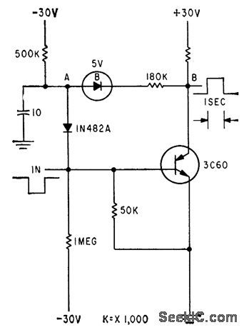
Provides up to 10 sec delay. Circuit is normally on, with point A at -11 v and B at +1 v. Negative trigger op plied to base of pnpn unit operates circuit.-J. B. Hangstefer and L. H. Dixon, Jr., Triggered Bistable Semiconductor Circuits, Electronics, 32:35, p 58-60. (View)
View full Circuit Diagram | Comments | Reading(674)
MINIATURE_WIDEbAND_AMPLIFIER
Published:2009/7/7 7:53:00 Author:May
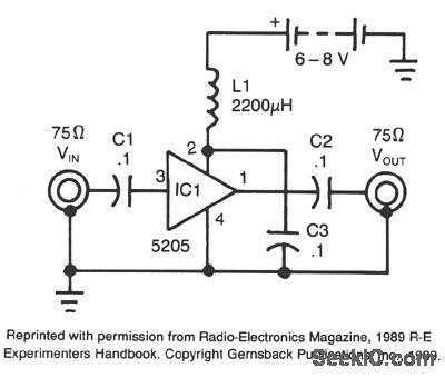
This wideband amplifier uses only five compo-nents. External signals enter pin 3 of IC1 via ac coupling capacitor C1. Following amplification, the boosted signals from IC1 pin 1 are coupled to the output by capacitor C2. Capacitor C3 decouples the dc power supply, while rf current is isolated from the power supply by rf choke L1.The NE5205's low current consumption of 25 mA at 6 Vdc makes battery-powered operation a reality. Although the device is rated for a 6 to 8 V power supply, 6 V is recommended for normal operation. From 6 V an internal bias of 3.3 V results, which permits a 1.4 V pk-pk output swing for video applications. (View)
View full Circuit Diagram | Comments | Reading(0)
BROADCAST_BAND_RF_AMPLIFIER
Published:2009/7/7 7:50:00 Author:May

The circuit has a frequency response ranging from 100 Hz to 3 MHz;gam is about 30 dB,Field-effecttransistor Q1is configured In the coΠ1mon-source self-biased mode. Optional resistor R1 allows you to setthe input impedance to any desired value;commonly,it will be 50 Ω.The signalis then direct coupled to Q2, a common-base circuit that isolates the input and outputstages and provides the amplifier’s exceptional stability. Last, Q3 functions as an emitter follower, to provide low output impedance at about 50 Ω.If you need higher output impedance,include resistor R8. It willaffect impedance according to this formula:R8≈ROUT -50. Otherwise,connect output capacitor C4directly to the emitter of Q3. (View)
View full Circuit Diagram | Comments | Reading(3126)
WIDEBAND_UHF_AMPLIFIER_WITH_HIGH_PERFORMANCE_FETS
Published:2009/7/7 7:46:00 Author:May
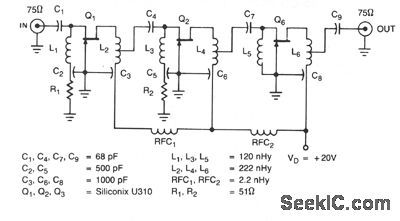
The amplifier circuit is designed for a 225 MHz center frequency, 1 dB bandwidth of 50 MHz, low-input VSWR in a 75-Ω system, and 24 dB gain. Three stages of U310 FETs are used, in a straight-forward design. (View)
View full Circuit Diagram | Comments | Reading(0)
28_dB_NONINVERTING_AMPLIFIER
Published:2009/7/7 7:42:00 Author:May
The physical circuit layout is extremely critical. Breadboarding is not recommended. A double-sided copper-clad printed circuit board will result in more favorable system operation. (View)
View full Circuit Diagram | Comments | Reading(517)
29_MHz_AMPLIFIER
Published:2009/7/7 7:40:00 Author:May
The only adjustments that require close attention are input, output, and neutralization. The 150-pF capacitor in the input line compensates for impedance mismatch. You tune for maximum signal transfer from exiter to final with an in-line meter or external field strength meter. The final is a conventional pi network. When neutralized, the plate current dip should be at about the same setting of the 20-pF plate capacitor as maximum output. Adjust bias to let tubes idle at about 30 mA. (View)
View full Circuit Diagram | Comments | Reading(565)
80_W_PEP_3_30_MHz_125_136_V_AMPLIFIER
Published:2009/7/7 7:39:00 Author:May
This amplifier utilizes a 2N6367 and a pair of 2N6368 transistors. The 2N6367 transistor is employed as a driver and is specified for up to 9 W (PEP) output. In the amplifier design the driver must supply on 5 W (PEP) at 30 MHz with a resulting IMD performance of about -37 to -38 dB. At lower operating fre-quencies, drive requirements drop to the 2-3 W (PEP) range and IMD performance improves to better than 40 dB. Two 2N6368 transistors are employed in the final stage of the transmitter design in a push-pull configuration. These devices are rated at 40 MI (PEP) and -30 dB maximum IMD, although -35 dB per-formance is more typical for narrowband operation. Without frequency compensation, the completed amplifier can deliver 90W (PEP) in the 25-30 MHz band with IMD performance down -30 dB. If only the power amplifier stage is frequency compensated, 95 W (PEP) can be obtained at 6- 10 MHz. (View)
View full Circuit Diagram | Comments | Reading(1076)
2_30_MHz_140_W_PEP_AMATEUR_RADIO_LINEAR_AMPLIFIER
Published:2009/7/7 7:36:00 Author:May

He amplifier operates across the 2-30 MHz band with relatively flat gain response and reaches gain saturation at approximately 210 W of output power. Both input and output transformers are 4:1 turns ratio (16:1 impedance ratio) to achieve low input SWR across the specified band and a high saturation capability.When using this design, it is important to interconnect the ground plane on the bottom of the board to the top, especially at the emitters of the MRF454s. (View)
View full Circuit Diagram | Comments | Reading(668)
| Pages:109/250 At 20101102103104105106107108109110111112113114115116117118119120Under 20 |
Circuit Categories
power supply circuit
Amplifier Circuit
Basic Circuit
LED and Light Circuit
Sensor Circuit
Signal Processing
Electrical Equipment Circuit
Control Circuit
Remote Control Circuit
A/D-D/A Converter Circuit
Audio Circuit
Measuring and Test Circuit
Communication Circuit
Computer-Related Circuit
555 Circuit
Automotive Circuit
Repairing Circuit