
Amplifier Circuit
Index 111
DEMONSTRATION_COMPARATOR_CIRCUIT
Published:2009/7/7 4:05:00 Author:May
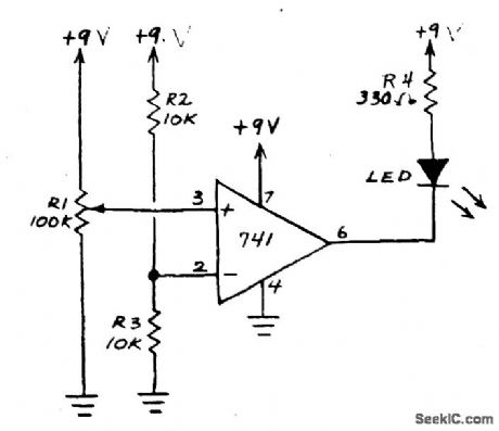
This circuit is an op amp without a feedback resistor. R2 and R3 junction point sets the reference voltage. When the input voltage set by R1 is below the reference voltage the LED glows. If voltage is above reference, the LED goes off. (View)
View full Circuit Diagram | Comments | Reading(1691)
FREQUENCY_COMPARATOR
Published:2009/7/7 4:04:00 Author:May
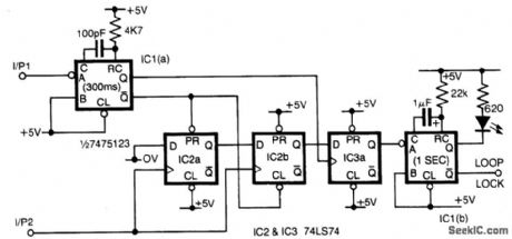
Input 1 is used as a gating period, during which a single rising edge on input 2 will cause a logic 1 output-any other number, indicating non-identical frequencies causes a logic 0 output. IC1a converts input 1 to a narrow pulse which initializes IC2 which forms a two-stage shift register clocked by input 2. On the first edge of input 2 a logic 1 appears on the output of IC2b and for all subsequent inputs a logic 0 is present. At the end of the gating period this output is latched by IC3 forming the lock output. As this is only valid for one input period a monostable is added to the output to enable, for example, visual monitoring of the output. Either output from IC3 can be used depending on which state is most important. As connected the failure state is indicated. (View)
View full Circuit Diagram | Comments | Reading(0)
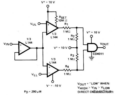
HIGH_INPUT_IMPEDANCE_WINDOW_COMPARATOR
Published:2009/7/7 4:02:00 Author:May
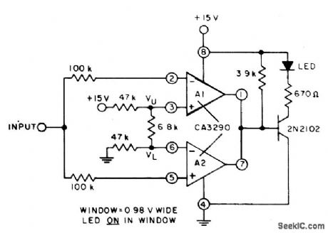
The circuit uses both halves of the CA3290 BiMOS dual voltage comparator. The LED will be turned 0N whenever the input signal is above the lower limit (VL) but below the upper limit (VU). (View)
View full Circuit Diagram | Comments | Reading(573)
HIGH_LOW_LEVEL_COMPARATOR_WITH_ONE_OP_AMP
Published:2009/7/7 4:00:00 Author:May
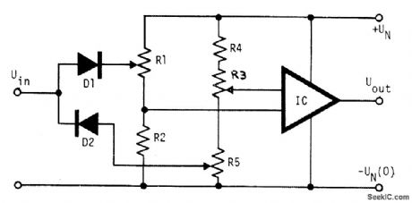
The voltage to be compared is fed through diode D1 and D2 to the voltage dividers R1 and R5 where the low and high limits are present. When the voltage level of an input signal exceeds the high threshold limit set with potentiometer R1, the diode D1 becomes forward biased and the increased voltage on the inputs of the op amp drives it into positive saturation. Similarly, a decrease of the input voltage at the op amp inputs turns the op amp to positive saturation. Potentiometer R3 is used for zeroing the op amp in the off state. (View)
View full Circuit Diagram | Comments | Reading(743)
WINDOW_COMPARATOR
Published:2009/7/7 3:56:00 Author:May
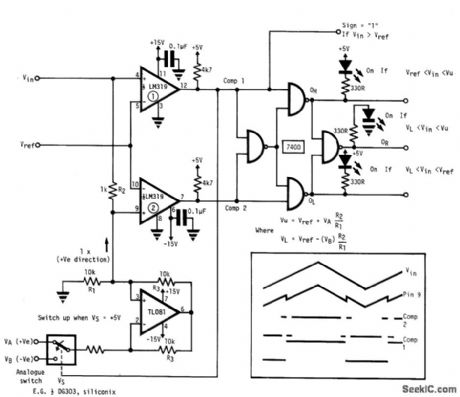
This circuit provides independently adjustable upper and lower threshold settings, and has sign, in window range, in upper window, and in lower window digital outputs. (View)
View full Circuit Diagram | Comments | Reading(0)
LOW_CPST_COMPARATOR_AND_DISPLAY
Published:2009/7/7 3:54:00 Author:May

An op amp is used as a comparator and a sink for LED current. The output voltage of the amplifier changes about 1.4 V depending on the direction of the current. Only one transistor is on at any time. Maximum LED current is limited to 25 mA by overcurrent protection of the μA741. If LEDs are not Capable of carrying such a current or an alternative op amp is used and an additional resistor Rlim is necessary. (View)
View full Circuit Diagram | Comments | Reading(544)
DOUBLE_ENDED_LIMIT_COMPARATOR
Published:2009/7/7 3:52:00 Author:May
View full Circuit Diagram | Comments | Reading(0)
LIMIT_COMPARATOR
Published:2009/7/7 3:50:00 Author:May
View full Circuit Diagram | Comments | Reading(0)
VOLTAGE_MONITOR_COMPARATOR
Published:2009/7/7 3:49:00 Author:May

A portion of the monitored voltage (deter-mined by R1's adjustment) is compared to a fixed voltage obtained from a zener reference network, R2-D1. As long as the monitored volt-age remains at or above its present monitor point (determined by R1's setting), the output indicator, LED1, remains dark. If the voltage drops below this level, the LED goes on. D1 is a 3.3-V zener. A 12 Vdc power supply is suitable for monitoring input voltages of up to 12 volts. (View)
View full Circuit Diagram | Comments | Reading(843)
LOW_POWER_COMPARATOR_WITH_LESS_THAN_10_μV_HYSTERESIS
Published:2009/7/7 3:47:00 Author:May
View full Circuit Diagram | Comments | Reading(520)
PULSE_TRAIN_AMPLITUDE_MODULATOR
Published:2009/7/22 1:13:00 Author:Jessie

Provides amplitude modulation of pulse train with audio signal or other input, such as noise, over range of 0 to 200 kc with :input pulses over 1 microsec wide,80% modulalation is available up to 3 kc, decreasing to 30% at input of 200 kc,-J. F. McCormick,Jr, Pulse Amplitude Modulator, EEE. 13:7,p 44. (View)
View full Circuit Diagram | Comments | Reading(2724)
VHF_TRANSISTOR_AMPLIFIER_TESTER
Published:2009/7/21 22:26:00 Author:Jessie

Has 6xed match, neutralization, and bias for use as standard test circuit for transistors in tv or vhf r-f amplifier stage. With 2N1742 transistor, power gain is 19 db, bandwidth up to 16 Mc, and maximum noise 5.5 db. -G. J. Flynn, Engineering Trends in Consumer Electronics, Electronics, 34:1, p 115-117. (View)
View full Circuit Diagram | Comments | Reading(594)
Four_stage_ring_counter_using_SUS_devices
Published:2009/7/21 22:17:00 Author:Jessie

Four-stage ring counter using SUS devices (courtesy Motorola Semiconductor Products Inc.). (View)
View full Circuit Diagram | Comments | Reading(875)
CRYSTAL_BFO
Published:2009/7/21 22:14:00 Author:Jessie

Bipolar crystal oscillator is coupled to FET source-follower by miniature 455-kHz IF transformer T2. RF output is adjusted with R7A so BFO injection voltage can be set for maximum carrier suppression. BFO is 456.35 kHz for lower sideband operation or 453.75 kHz for upper sideband in SSB transceiver.-W. J. Weiser, Integrated Circuit SSB Transceiver for 80 Meters, Ham Radio, April 1976, p 48-52. (View)
View full Circuit Diagram | Comments | Reading(3578)
THERMOCOUPLE_AMPLIFIER_WITH_COLD_JUNCTION_COMPENSATION
Published:2009/7/7 2:43:00 Author:May

Input protection circuitry allows thermocouple to short to 120 Vac without damaging the amplifier.
Calibration: 1. Apply a 50 mV signal in place of the thermocouple. Trim R3 for VOUTut 12.25 V. 2. Reconnect the thermocouple. Trim R9 for correct output. (View)
View full Circuit Diagram | Comments | Reading(0)
LOW_VOLTAGE_COMPANDER
Published:2009/7/7 1:36:00 Author:May

The NE575 is a dual-gain control circuit designed for low voltage applications. The NE575's channel 1 is an expander, while channel 2 can be configured either for expander, compressor,or automatic level controller (ALC) applications. (View)
View full Circuit Diagram | Comments | Reading(1949)
FOUR_QUADRANT_MULTIPLIER
Published:2009/7/6 23:43:00 Author:May

Provides amplitude modulation for applications where low power consumption is more important than accuracy. Uses CA3080A variable opamp in combination with transistors of CA3018A array and 2N4037 amplifier for bias current of opamp. Ac-curacy is within 7% full scale.- Circuit Ideas for RCA Linear ICs, RCA Solid State Division, Somerville, NJ, 1977, p 15. (View)
View full Circuit Diagram | Comments | Reading(1676)
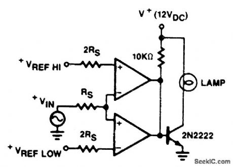
FOUR_CHANNEL_COMPARATOR
Published:2009/7/6 21:40:00 Author:May
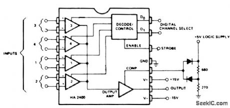
When operated as an open loop without compensation, the HA-2400 becomes a comparator with four selectable input channels. The clamping network at the compensation pin limits the output voltage to allow DTL or TTL digital circuits to be driven with a fanout of up to ten loads.
The circuit can be used to compare several signals against each other or against fixed references; or a single signal can be compared against several references. A window comparator, which assures that a signal is within a voltage range, can be formed by monitoring the output polarity, while rapidly switching between two channels with different reference inputs and the same signal input. (View)
View full Circuit Diagram | Comments | Reading(606)
WINDOW_COMPARATOR_1
Published:2009/7/6 21:39:00 Author:May
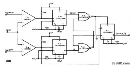
This window comparator generates an output pulse for each event that occurs within a specified window. That is, each output pulse signifies an input voltage pulse or level change that exceeds VREFLOW, but not VREFHIGH. The monostable multi ibrators, IC2A and IC2B, produce a 10-μS pulse at their Q output in response to a rising edge at their A input. Comparator IC1B produces a rising edge when the input exceeds VREFLOW, and comparator IC2A produces a rising edge when the input exceeds VREFHIGH. The NOR gates, IC3A and IC3B, form a bistable latch whose Q output, when low, disables IC4. IC4, unless disabled, produces output pulses in response to falling edges at the IC1B comparator output. You set the width of these pulses by selecting the value of C3. The circuit can handle an input waveform containing 0 to 2 V amplitudes and 10-Hz to 10-kHz frequency components. (View)
View full Circuit Diagram | Comments | Reading(0)
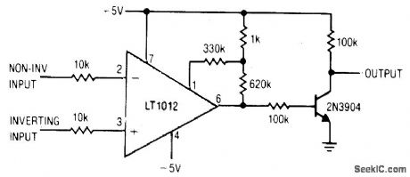
DUAL_LIMIT_MICROVOLT_COMPARATOR
Published:2009/7/6 21:35:00 Author:May

When the upper or lower limit is exceeded, the LED lights up. Positive feedback to one of the nulling terminals creates 5 to 20 μV of hysteresis on both amplifiers. This feedback changes to offset voltage of the LT1002 by less than 5μV . Therefore, the basic accuracy of the comparator is limited only by the low offset voltage of the LT1002.
(View)
View full Circuit Diagram | Comments | Reading(658)
| Pages:111/250 At 20101102103104105106107108109110111112113114115116117118119120Under 20 |
Circuit Categories
power supply circuit
Amplifier Circuit
Basic Circuit
LED and Light Circuit
Sensor Circuit
Signal Processing
Electrical Equipment Circuit
Control Circuit
Remote Control Circuit
A/D-D/A Converter Circuit
Audio Circuit
Measuring and Test Circuit
Communication Circuit
Computer-Related Circuit
555 Circuit
Automotive Circuit
Repairing Circuit