
Amplifier Circuit
Index 112
PRECISION_COMPARATOR_WITH_BALANCED_INPUTS_AND_VARIABLE_OFFSET
Published:2009/7/6 21:33:00 Author:May

View full Circuit Diagram | Comments | Reading(709)
FREQUENCY_DETECTING_COMPARATOR
Published:2009/7/6 21:30:00 Author:May

A quad comparator forms the basis of a frequency detector that is faster and less expensive than more complex versions designed around frequency-to-voltage converter chips. Positive feedback through a 5-MΩ resistor allows the circuit to resolve changes as small as two percent; the output responds to those changes in about one cycle. When the input frequency is high, V2 is pulled low; it's never allowed to exceed 2/3 V. When the input frequency is lower than the limit, V2 exceeds 2/3 V once each cycle, but V3 is held below that limit. The trip frequency is defined by F = 1/(1.1R2C2). R2 can be adjusted to permit trimming of the trip point, but the value of R3 must remain larger than R2. (View)
View full Circuit Diagram | Comments | Reading(773)
COMPARATOR_LATCH
Published:2009/7/6 21:27:00 Author:May

The primary advantage of this circuit, when compared to other comparators, is its ability to latch after the input has reached a predetermined threshold level. When the input exceeds the threshold level, the LM311N output increases.This transition enables the strobe input, preventing the output from falling low. A high-level voltage on the reset input will turn off Q1, thereby removing the supply voltage from the open collector output of the LM311N. With no supply to the strobe input, the latch condition is removed and the output is again allowed to follow the input excursions. The LM311N will operate with a wide variety of supply voltage levels, ranging from dual ±15 V to a single 5 V level that provides compatibility with digital IC logic. If more than one latch is used with a common reset, all the pull-up resistors may be connected to Q1's collector. (View)
View full Circuit Diagram | Comments | Reading(2765)
MICROVOLT_COMPARATOR_WITH_HYSTERESIS
Published:2009/7/6 21:26:00 Author:May

Positive feedback to one of the nulling terminals creates approximately 5 μV of hysteresis. The output can sink 16 mA; the input offset voltage is typically changed less than 5μV because of the feedback. (View)
View full Circuit Diagram | Comments | Reading(771)
WINDOW_COMPARATOR
Published:2009/7/6 21:25:00 Author:May

A window detector is a specialized comparator circuit designed to detect the presence of a voltage between two prescribed limits; that is, within a voltage window. This circuit is implemented by logically combining the outputs of two single-ended comparators by the IN914 diodes. When the input voltage is between the upper limit, VUL, and the lower limit, VLL, the output voltage is zero; otherwise it equals a logic high level. The output of this circuit can be used to drive a logic gate, LED driver, or relay driver circuit. The circuit shown in Fig. 16-1 shows a 2N2222 npn transistor being driven by the window comparator. When the input voltage to the window comparator is outside the range set by the VUL and VLL inputs, the output changes to positive, which turns on the transistor and lights the LED indicator.
(View)
View full Circuit Diagram | Comments | Reading(0)
CHARGE_COMPENSATED_SAMPLE_AND_HOLD
Published:2009/7/6 21:15:00 Author:May

Circuit NotesLess than±5 pC charge transfer(less than 5 mV sample-to-hold offset when CL=1000 pF). (View)
View full Circuit Diagram | Comments | Reading(668)
SYNCHRONIZING__TWO__MICROPROCES_SORS
Published:2009/7/6 21:15:00 Author:May

4-MHz oscillator using 74LS00 quad two-input NAND gates serves in place of crystal source of individual MC6802 microprocessors to ensure synchronizing so one microprocessor operates during half-cycle when other microprocessor is disabled Arrangement gives computing power of two MPUs with system cost of one data bus. No time is sacrificed since half-cycle used would normally be dead time on bus.-J. Farrell, “Synchronizing Two Motorola MC6802s on One Bus,” Motorola, Phoenix, AZ,1978, AN-783. (View)
View full Circuit Diagram | Comments | Reading(820)
INFINITE_SAMPLE_AND_HOLD_AMPLIFIER
Published:2009/7/6 21:12:00 Author:May

Circuit NotesDuring normal hold mode, the replicated analog voltage is buffered straight through the S/H amplifier to the output. Upon issuance of a SAMPLE signal, the SiH amplifier is placed in the hold mode, holding the voltage until the new analog voltage is valid. The same SAMPLE signal triggers an update to the input sample-and-hold amplifier. The most current analog voltage is captured and held for conversion. The previously deter-mined voltage is held stable at the output during the conversion cycle while the SAR/D-to-A converter continuously adjusts to replicate the new input voltage. At the end of the conversion, the output sample-and-hold amplifier is once again placed in the track mode. The new analog voltage is then regenerated. (View)
View full Circuit Diagram | Comments | Reading(729)
SINGLE_OP_AMP_CLOCK
Published:2009/7/6 21:05:00 Author:May

Capacitor C1 is charged through timing resistor R1 when the clock output is high. When C1 reaches the upper threshold voltage, the output signal decreases, and then C1 discharges through R1 until its voltage reaches the lower threshold point. When this happens, the output increases again and the cycle repeats itself. Using the parts values shown results in a frequency of 1 Hz. The output frequency can be adjusted by trimming the value of R1 slightly. (View)
View full Circuit Diagram | Comments | Reading(724)
AF_SQUELCH_AMPLIFIER
Published:2009/7/22 1:18:00 Author:Jessie

Holds audio channel of receiver silent until receiver input signal reaches predetermined amplitude. DC control voltage can be derived from IF amplifier by rectification or from second detector of receiver. FET is biased to cutoff by DC gate voltage applied to threshold terminals. DC control voltage bucks this bias and activates amplifier when-ever it exceeds predetermined threshold in range of 0-6 V. If receiver gives opposite polarity for DC voltages, use P-channel FET such as 2N2608, reverse C2, and change R4 and R5 as required.-R. P. Turner, FET Circuits, Howard W. Sams, Indianapolis, IN, 1977, 2nd Ed., p 73-74. (View)
View full Circuit Diagram | Comments | Reading(811)
The principle circuit diagram of 915MHz intermediate power amplifier composed of RF2104
Published:2011/5/9 21:48:00 Author:May | Keyword: 915MHz, middle power, amplifier

The principle circuit diagram of 915MHz intermediate power amplifier composed of RF2104 is shown in the following diagram:
(View)
View full Circuit Diagram | Comments | Reading(731)
The Basic Circuit Diagram of 420MHz Intermediate Power Amplifier Composed of RF2104
Published:2011/5/13 4:53:00 Author:May | Keyword: 420MHz, Intermediate Power Amplifier

The Basic Circuit Diagram of 420MHz Intermediate Power Amplifier Composed of RF2104 is shown in the following diagram:
(View)
View full Circuit Diagram | Comments | Reading(812)
Optocoupler_that_is_used_to_couple_ac_to_an_op_amp
Published:2009/7/22 21:59:00 Author:Jessie
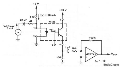
In this circuit, the LED portion of the 4N26 is biased with a dc current of 10 mA. The input ac signal is summed with the dc bias so that the 4N26 output has both ac and dc components. Because the op amp is capacitively coupled to the 4N26, only the ac signal appears at the op-amp output. (View)
View full Circuit Diagram | Comments | Reading(3455)
GRAPHICS_INTERFACE
Published:2009/7/6 20:49:00 Author:May
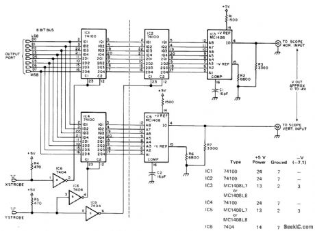
Used between computer and ordinary CRO to create images with array of 512 x 512 dots stored in computer memory. Location of each dot is specified by two voltages, for application to V and H inputs of CRO. Computer provides voltage values by outputting two binary words to pair of DACs giving voltages proportional to numerical values of words. Dot pattern is repeated many times per second to give steady nonflickering image. Dot brightness can be increased by storing in several locations so it is refreshed more often than other points. Article gives listing for Intel 8080 graphics drive program. Program pro-vides for interrupts once per scan to give key-board-controlled drawing mode,-P. Nelson, Build the Beer Budget Graphics Interface, BYTE, Nov. 1976, p 26-29. (View)
View full Circuit Diagram | Comments | Reading(723)
Op_amp_circuits_titles_and_descriptions
Published:2009/7/22 22:36:00 Author:Jessie
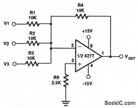
Because R1 through R4 are all the same value, VOUT=V1+V2+V3. Notice that R6 equals the parallel resistance of R1 through R4 and VOUT= -R4. (View)
View full Circuit Diagram | Comments | Reading(698)
Optically_coupled_Schmitt_trigger
Published:2009/7/22 22:07:00 Author:Jessie
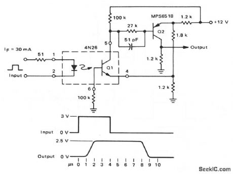
This circuit uses the 4N26 transistor as part of a Schmitt trigger. When Q1 conducts in response to an input pulse, Q2 conducts and the output is high.When the input pulse is removed from the 4N26, Q1 shuts off, and the output is low. With the values shown, the tum-off delay is about 2 μs, and the turn-off delay is about 6 ps. Speed can be improved by lowering the value of the Q1 base resistance from 100 kΩ, but the drive requirements must be increased. (View)
View full Circuit Diagram | Comments | Reading(2130)
VOLTAGE_FOLLOWER
Published:2009/7/6 9:33:00 Author:May
View full Circuit Diagram | Comments | Reading(0)
SIMPLE_FOLLOWER
Published:2009/7/6 9:33:00 Author:May
View full Circuit Diagram | Comments | Reading(532)
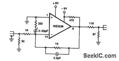
HIGH_FREQUENCY_NONINVERTING_FOLLOWER
Published:2009/7/6 9:33:00 Author:May
View full Circuit Diagram | Comments | Reading(591)
HIGH_FREQUENCY_INVERTING_FOLLOWER
Published:2009/7/6 9:32:00 Author:May
View full Circuit Diagram | Comments | Reading(733)
| Pages:112/250 At 20101102103104105106107108109110111112113114115116117118119120Under 20 |
Circuit Categories
power supply circuit
Amplifier Circuit
Basic Circuit
LED and Light Circuit
Sensor Circuit
Signal Processing
Electrical Equipment Circuit
Control Circuit
Remote Control Circuit
A/D-D/A Converter Circuit
Audio Circuit
Measuring and Test Circuit
Communication Circuit
Computer-Related Circuit
555 Circuit
Automotive Circuit
Repairing Circuit