
Amplifier Circuit
Index 101
DIFFERENTIAL_PREAMP
Published:2009/7/9 5:23:00 Author:May

Opamps A1 and A2 form cross-coupled preamp with differential input and differential output, driving instrumentation opamp A3 to provide overall gain of 106. Common-mode input range is ±10 V, and full.scale differential input is ±100 mV. For higher input impedance, 108 opamps can be used in preamp. For higher speed, all three opamps can be 118.-W. G. Jung, IC 0p-Amp Cookbook, Howard W. Sams, Indianapolis, IN, 1974, p 241-243. (View)
View full Circuit Diagram | Comments | Reading(1561)
HIGH_POWER_CAR_AUDIO_AMPLIFIER
Published:2009/7/9 5:21:00 Author:May
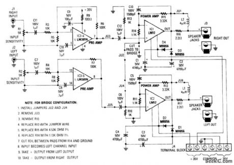
This stereo amp will supply 60 W rms into 8Ω or 100 W rms into 4Ω. Notice that the LM12C1 line level (about 300 mV) into 5 KΩ. A±35-V supply is required for full power output. Power can be obtained from a dc-dc converter. (View)
View full Circuit Diagram | Comments | Reading(1401)
15_watt_AF_power_amplifier_using_an_ECG1059_chip_and_two_ECG175_bipolar_transistors
Published:2009/7/20 4:38:00 Author:Jessie

15-watt AF power amplifier using an ECG1059 chip and two ECG175 bipolar transistors. Minimum voltage gain is 63 dB. Maximum input voltage is 1 mV for the given output (courtesy GTE Sylvania Incorporated). (View)
View full Circuit Diagram | Comments | Reading(656)
High_gain_AF_preamplifier_using_an_ECG1053_chip
Published:2009/7/20 4:37:00 Author:Jessie
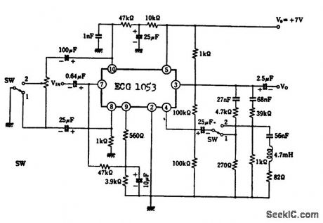
High-gain AF preamplifier using an ECG1053 chip. Frequency response is from 30 hertz to 15 kilohertz. Minimum voltage gain is 93 dB (courtesy GTE Sylvania Incorporated). (View)
View full Circuit Diagram | Comments | Reading(705)
2_watt_AF_power_amplifier_for_a_16_ohm_load_using_a_GEIC_1
Published:2009/7/20 4:35:00 Author:Jessie
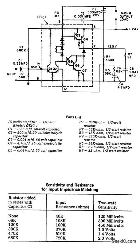
2-watt AF power amplifier for a 16-ohm load using a GEIC-1. See table for sensitivity (courtesy General Electric Company). (View)
View full Circuit Diagram | Comments | Reading(543)
AUTOMOBILE_LIGHTS_ON_REMINDER
Published:2009/7/9 5:07:00 Author:May
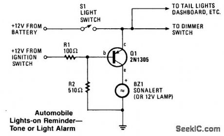
The circuit can be used to give a visible or an audible warning that the headlights are on. It uses a 2N1305 transistor as a switch to tum on a Sonalert tone generator or a small 12-V lamp. Operating current for the transistor is supplied from the wire that feeds the headlights. When the ignition is on, the transistor is biased off and the alarm is not activated. Turning off the ignition while the lights are on sets off the alarm. (View)
View full Circuit Diagram | Comments | Reading(924)
2_watt_AF_power_amplifier_with_8_ohm_load_connected_to_supply
Published:2009/7/20 4:32:00 Author:Jessie
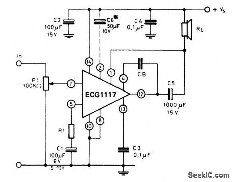
2-watt AF power amplifier with 8-ohm load connected to supply. Rated output of 2 watts is obtained with a supply voltage of 12volts with an 8-ohm load. At 9volts with the same 8-ohm load a rated output of 1.2 watts is obtained. At 9 volts with a 4-ohm load power output is rated at 1.6 watts. Capacitor 06 must be used when high ripple rejection is required. The ECG1117 is a 14-pin QIP (courtesy GTE Sylvania Incorporated). (View)
View full Circuit Diagram | Comments | Reading(596)
20__40__50__60_watt_complementary_Darlington_AF_power_amplifier
Published:2009/7/20 5:23:00 Author:Jessie
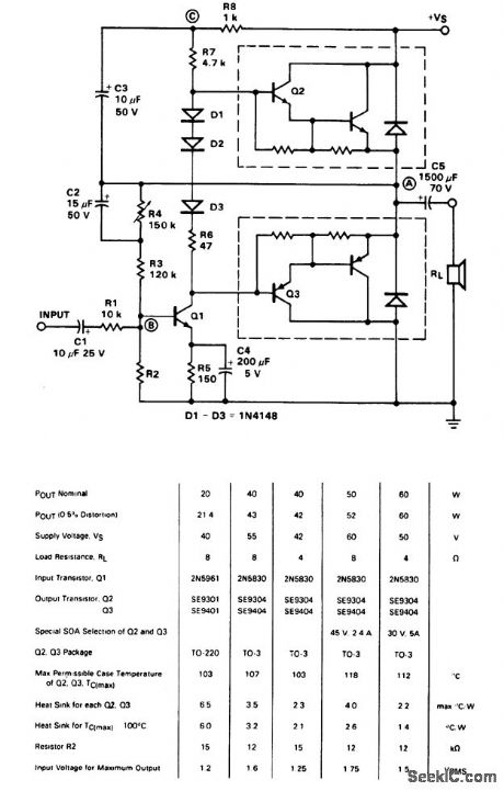
20-/40-/50-/60-watt complementary Darlington AF power amplifier. See table for amplifier component specs (courtesy Fairchild Semiconductor). (View)
View full Circuit Diagram | Comments | Reading(1050)
58_watt_AF_power_amplifier_for_automotive_applications
Published:2009/7/20 5:20:00 Author:Jessie
5.8-watt AF power amplifier for automotive applications. This circuit is ideal for car stereo or car radio outputs. In addition it can be employed for a CB modulator circuit. Recommended supply voltage is 13.2 volts. Input resistance is 40K. Voltage gain ranges between 52 and 58 dB (courtesy GTE Sylvania Incorporated). (View)
View full Circuit Diagram | Comments | Reading(610)
500_mW_AF_power_amplifier_for_a_20_ohm_speaker
Published:2009/7/20 5:19:00 Author:Jessie

500 mW AF power amplifier for a 20-ohm speaker. Frequency response is from 70 hertz to 20 kilohertz. The ECG1016 is a thin-film hybrid module. The AF driver transistor is standard and can be purchased en Radio Shack (courtesy GTE Sylvania Incorporated). (View)
View full Circuit Diagram | Comments | Reading(767)
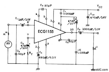
4_watt_audio_power_amplifier_using_an_ECG1102_as_an_AF_driver
Published:2009/7/20 5:11:00 Author:Jessie
4-watt audio power amplifier using an ECG1102 as an AF driver. The ECG1102 is a 5-pin module. The two bias pots in the output stage should be adjusted to provide an idle current of 15 mA. Total current at maximum output is 450 mA. Voltage gain is 28 dB. Bandwidth is from 20 hertz to 30 kilohertz (courtesy GTE Sylvania Incorporated). (View)
View full Circuit Diagram | Comments | Reading(679)
250_mW_babysitter_intercom_using_an_LM3909_chip
Published:2009/7/20 5:10:00 Author:Jessie
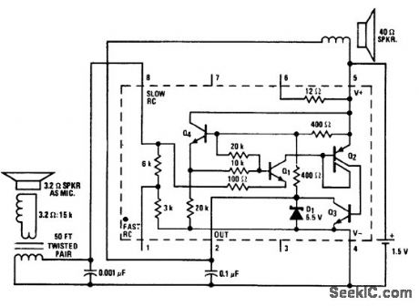
250 mW babysitter intercom using an LM3909 chip. Circuitry inside dashed lines is the LM3909. Operating current is 12to 15mA (courtesy National Semiconductor Corporation). (View)
View full Circuit Diagram | Comments | Reading(673)
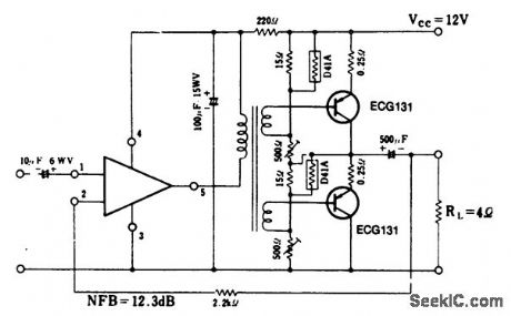
15_watt_20_watt_AF_amplifier_using_complementary_Darlington_output_transistors
Published:2009/7/20 5:08:00 Author:Jessie

15-watt/20-watt AF amplifier using complementary Darlington output transistors. To ensure maximum signal swing the junction of R8 and R9 should be half-Voc (courtesy Motorola Semiconductor Products Inc.). (View)
View full Circuit Diagram | Comments | Reading(1899)
1_Hz_TIMEBASE_FOR_READOUT_AND_COUNTER_APPLICATIONS
Published:2009/7/9 4:08:00 Author:May
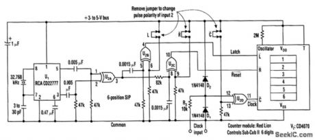
This counter makes direct readout of frequency-generating equipment very easy when a 1-Hz time-base is added to latch, reset, and the count signal is conditioned. This design has the flexibility to select either polarity.
By differentiating, inverting, and ORing the clock pulses in XOR gate U2A, a stream of 1-Hz, positive, 200-μs pulses is generated. For latching, the 1-Hz stream is again differentiated in U2B, input 1 to supply a 50-μs pulse. Though U2B's output goes from high to low, it can be reversed, by making input 2 low.
Because the reset pulse must occur after the latch signal, the 1-Hz stream from U2A is delayed 100 μs at U2C input 1. The output-pulse polarity is determined by making U2C's input 2 either high or low. (View)
View full Circuit Diagram | Comments | Reading(818)
GENERAL_PURPOSE_PREAMP
Published:2009/7/9 3:35:00 Author:May
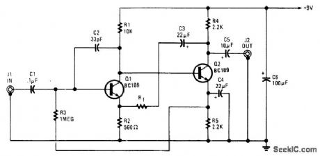
This amplifier is useful for audio and video applications. Gain is set by Rf and the voltage gain of this amplifier is approximately 1 +Rf/560, where Rf is in ohms. Bandwidth depends on gain selected, but typi-cally it is several MHz. Rf=5.1 kΩ, which produces a gain of 10x (20 dB) voltage. (View)
View full Circuit Diagram | Comments | Reading(1102)
MICROPHONE_PREAMP_
Published:2009/7/9 3:34:00 Author:May
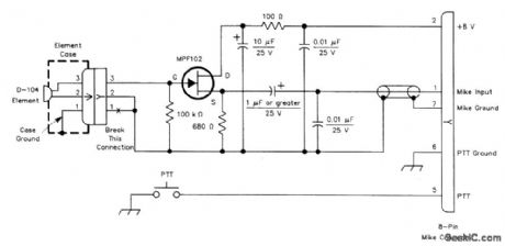
This circuitis used to interface a high-impedance microphone to a radio transceiver that requires alow-impedance microphone.The supply voltage can be either a battery or taken from the transceiver thecircuit is used with. (View)
View full Circuit Diagram | Comments | Reading(871)
LOW_IMPEDANCE_MICROPHONE_PREAMP
Published:2009/7/9 3:27:00 Author:May

This amplifter uses a common-gate FET amplifter to match a low-Z microphone. (View)
View full Circuit Diagram | Comments | Reading(1079)
LOW_FORWARD_DROP_RECTIFIER_CIRCUIT
Published:2009/7/9 3:27:00 Author:May
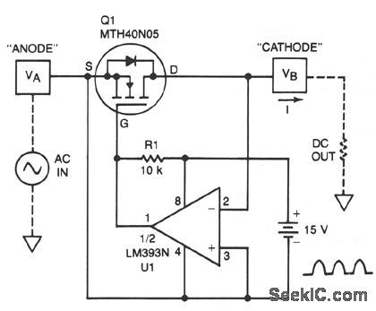
A TMOS power FET, Q1, and an LM393 comparator provide a high-efficiency rectifter circuit. When VA exceeds VB, U1's output becomes high and Q1 conducts. Conversely, when VB exceeds VA, the comparator output becomes low and Q1 does not conduct.The forward drop is determined by Q1's on resistance and current I. The MTH40N05 has an on resistance of 0.028 Ω; for I = 10 A, the forward drop is less than 0.3 V. Typically, the best Schottky diodes do not even begin conducting below a few hundred mV. (View)
View full Circuit Diagram | Comments | Reading(2299)
LOW_NOISE_AUDIO_PREAMP
Published:2009/7/9 3:26:00 Author:May
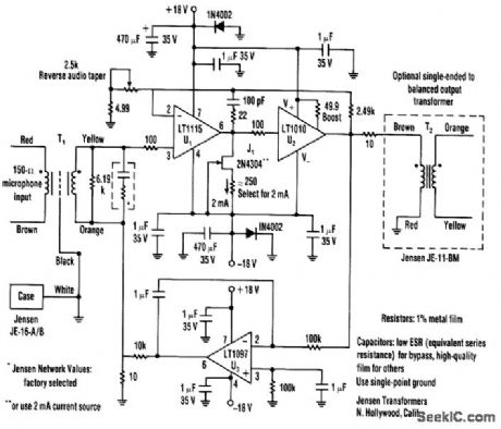
A low-noise LT1115 (Linear Technology, Inc.) op amp is coupled to class-A buffer amplirier to produce a variable gain (12-to-50 dB) microphone preamp. THD is less than 0.01% from 80Hz to over 20kHz. The transformers must be properly grounded and shielded. (View)
View full Circuit Diagram | Comments | Reading(2266)
CD4O49_AMPLIFIER
Published:2009/7/9 3:20:00 Author:May

When an inverter is biased with one resistor from its input to output in the range of 100 kΩ to 10 MΩ and is capacitor coupled, it exhibits amplifier characteristics (see the table).
Furthermore, when a split power-supply bus is needed and only one battery is used, the inverter can be configured to supply a pseudo-dc ground of relatively low impedance, coincident with the ac ground (see the ftgure). Depending on the magnitude of the dc ground return currents, anywhere from one inverter to several in parallel are sufficient. Also, the supply buses must be capacitor bypassed.
The configured inpqt-to-input shorted inverter now acts as a voltage regulator that sinks and sources current. In this configuration, the inverter is forced to operate at the midpoint of its transfer characteristic. This divides the battery potential into two equal parts-as referenced to the defined dc ground by virtue of its internal gain and physical structure. Op amps such as the LM324A, can be powered from one battery while being referenced to the dc ground that is generated by the inverter. This novel technique surpasses the use of discrete resistors for battery potential dividing. It can be employed in other applications where individual component savings and improved design performance are needed. (View)
View full Circuit Diagram | Comments | Reading(763)
| Pages:101/250 At 20101102103104105106107108109110111112113114115116117118119120Under 20 |
Circuit Categories
power supply circuit
Amplifier Circuit
Basic Circuit
LED and Light Circuit
Sensor Circuit
Signal Processing
Electrical Equipment Circuit
Control Circuit
Remote Control Circuit
A/D-D/A Converter Circuit
Audio Circuit
Measuring and Test Circuit
Communication Circuit
Computer-Related Circuit
555 Circuit
Automotive Circuit
Repairing Circuit