
Amplifier Circuit
Index 107
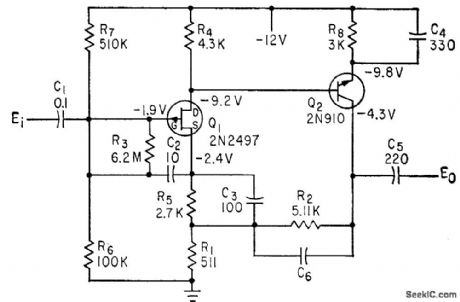
VLF_PREAMP_WITH_AGC
Published:2009/7/21 6:22:00 Author:Jessie
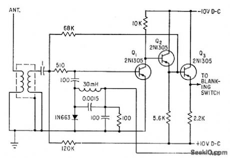
Fast-recovery computer diode acts as pure variable resistance shunting base of Q1 to ground, for full agc control without phase shift in output signal. In frequency range of 13 to 24 kc, phase shift is less than 0.25 microsec over 40-db input signal range.-J. D. Echols, Calibrating Frequency Standards with VLF Transmissions, Electronics, 35:17, p 60-63. (View)
View full Circuit Diagram | Comments | Reading(1003)
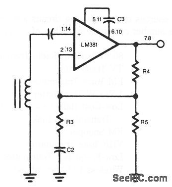
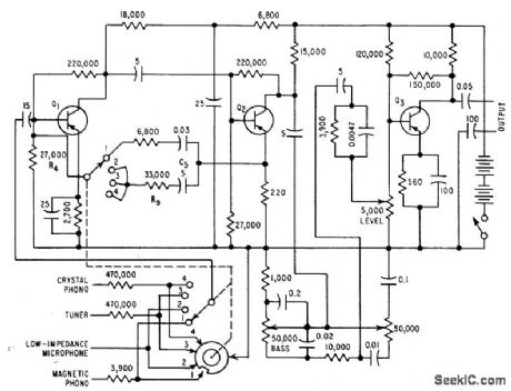
FLAT_RESPONSE_TAPE_AMPLIFIER
Published:2009/7/8 4:50:00 Author:May
View full Circuit Diagram | Comments | Reading(552)
MAGNETIC_PHONO_PREAMPLIFIER
Published:2009/7/8 4:49:00 Author:May

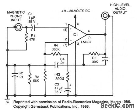
This simple stereo amplifier uses a National LM387IC. The piN numbers in parentheses are for one channel, and those not in parentheses are for the other channel. The supply voltage can be + 9 to + 30 Vdc at about 10 mA. The output voltage swing is about VCC-2 V pk-pk. The preamp should be able to deliver at least 5 V. (View)
View full Circuit Diagram | Comments | Reading(0)
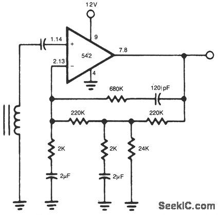
TWO_POLE_NAB_TYPE_PREAMP
Published:2009/7/8 4:46:00 Author:May

View full Circuit Diagram | Comments | Reading(504)
Battery_powered_load_cell_amplifier_for_discontinuous_service
Published:2009/7/21 3:16:00 Author:Jessie
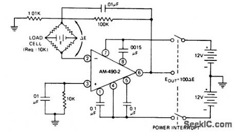
Battery-powered load-cell amplifier for discontinuous service. The AM-490-2 is an 8-pin TO-99 differential-input chopper-stabilized op amp. For power interrupt applications the amplifier has a warm-up period of 200 ms (courtesy Datel Systems, Inc.). (View)
View full Circuit Diagram | Comments | Reading(2577)
Differential_amplifier_using_a_Datel_AM_490_28_pin_TO_99_chip
Published:2009/7/21 3:15:00 Author:Jessie
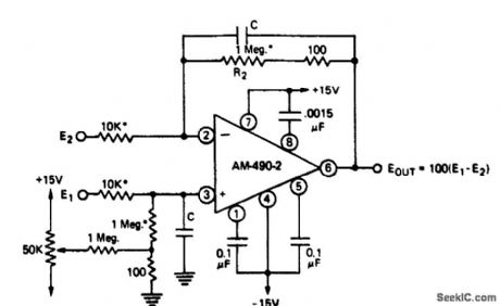
Differential amplifier using a Datel AM-490-28-pin TO-99 chip. For a 0.01% match between 1 M resistors and 10k resistors, common mode rejection ratio is approximately 120 dB. Capacitors Care used onlyto reduce bandwidth and hence output noise (courtesy Datel Systems, Inc.). (View)
View full Circuit Diagram | Comments | Reading(532)
NAB_RECORD_PREAMPLIFIER
Published:2009/7/8 4:45:00 Author:May

View full Circuit Diagram | Comments | Reading(577)
TAPE_PLAYBACK_AMPLIFIER
Published:2009/7/8 4:44:00 Author:May

View full Circuit Diagram | Comments | Reading(563)
_PWM_SERVO_AMPLIFIER
Published:2009/7/8 4:43:00 Author:May
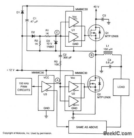
A major feature of the PWM servo amplifier is elimination of a pulse transformer. A 150 kHz pulse-width modulated signal is applied to U3, with its complementary outputs applied to identical circuits to drive the load. When point A increases, Q2 is on and point B is at ground potential. The VCC, for U1 is maintained through D1, and Q1 is held off by D2. When point A decreases,Q2 turns off, point C is pulled low by C2, which turns Q1 on. The time constant for R1, R3, and C2 can hold Q1 on just long enough to allow the voltage at point B to start rising. As point B rises, it charges C2 by forward biasing D3, maintaining point C low with respect to U1, and keeping Q1 turned on.
With point B at 40 V, D2 is off and point C is held low by R1 and R2, and VCC for U1 is maintained by the charge on C1. When point A increases again, Q2 again turns on, C2 pushes point C high, and turns Q1 off long enough to allow the voltage at point B to start falling. C2 is now discharged by reverse-biased D3, which keeps point C high with respect to U1, and keeps Q1 off. Once point B reaches ground potential, D1 again turns on, recharging C1, and maintaining VCC to U1. D2 also turns on and keeps Q1 off. (View)
View full Circuit Diagram | Comments | Reading(1070)
THERMOCOUPLE_AMPLIFIER
Published:2009/7/8 4:43:00 Author:May
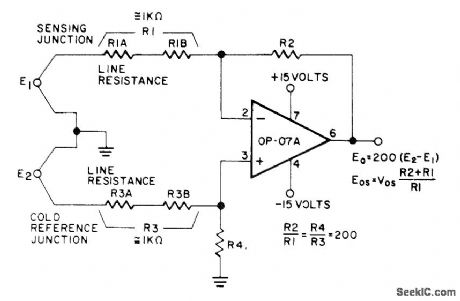
Precision Monolithics 0P-07A opamp has high common-mode rejection ratio and long-term accuracy required for use with thermocouples having full-scale outputs under 50 mV, frequently located in high-noise industrial environments. CMRR is 100 dB over full ±13 V range when ratios R2/R1 and R4/R3 are matched within 0.01'/0, Circuit is useful in many other applications where small differential signals from low-impedance sources must be accurately amplified in presence of large Gommon-mode voltages.—D.Soderquist and G Erdi, The op-07 Ultra-LowOffset voltage Op Amp-a Bipolar Op Amp That Challenges Choppers,Eliminates Nulling, Precision Monolithics, Santa Clara,CA,1975,AN-13,p 11.
(View)
View full Circuit Diagram | Comments | Reading(0)
PHOTODIODE_AMPLIFIER
Published:2009/7/8 4:43:00 Author:May

This circuit uses a CA5422 dual BiMOS microprocessor op amp. The bootstrap amplifiers minimize bias currents while maintaining electrostatic discharge protection. Additionally, the potentiometers and their associated resistors, R1 through R4, permit the user to trim bias currents to zero. (View)
View full Circuit Diagram | Comments | Reading(0)
DIFFERENTIAL-TO_SINGLE_ENDED_VOLTAGE_AMPLIFIER
Published:2009/7/8 4:38:00 Author:May
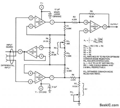
This circuit uses a CA5470 quad microprocessor BiMOS-E op amp. Amplifiers A1 and A2 are employed as a cross-coupled differential input and differential output preamp stage and A3 provides input guard-banding. Amplifier A4 converts the differential outputs of A and A2 to a single-ended output. (View)
View full Circuit Diagram | Comments | Reading(881)
1_W_EXCITER_FOR_7_AND_14_MHz
Published:2009/7/8 4:25:00 Author:May
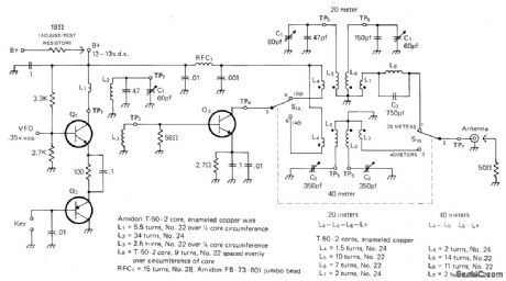
Developedfor use in simple solid-state VFO transmittercovering 40 and 20 meters for low-power operation Adequate drive can be provided by any 7-MHz VFO that develops 0.45 VRMS across 1000-ohm load. Circuit consists of olass A bufferl amplifier Q1 and keying switch Q2. Q3 is class C amplifier on 7 MHz (40m) and frequency doubler on 14 MHz (20m). Q1 is MPS6514. Q2 is 2N3906 or equivalent, Q3 is MPS-U31. All trans-former cores are Amidon T-50-2.—A. Weiss, QRP, CQ Nov. 1971, p 54-58 and 88. (View)
View full Circuit Diagram | Comments | Reading(806)
AM_FM_WITH_AGC_
Published:2009/7/8 4:10:00 Author:May

Operates from single +15 V supply. Standard 455-kHz IF is used for AM to feed 1N34A diode detector. One output of MC1350 is used for FM signal component and the other for AM component. External transistor is needed because MC1350 requires up to 0.2 mA of AGC drive and this is more than can be furnished by diode detector.- Integrated Circuit IF Amplifiers for AM/FM and FM Radios, Motorola,Phoenix, AZ, 1975, AN-543A, p 10.
(View)
View full Circuit Diagram | Comments | Reading(2709)
120_144_MHz
Published:2009/7/8 3:44:00 Author:May
General-purpose amplifier can be used around 120 MHz as microwave IF strip and up to 144 MHz for RF. Transistor type is not critical.-B. Hoisington, DC lsolation, 73 Magazine,Peterborough NH 03458,July 1974,p 55-62. (View)
View full Circuit Diagram | Comments | Reading(551)
FET_PNP_BOOTSTRAPPED_SOURCE_FOLLOWER_
Published:2009/7/21 6:07:00 Author:Jessie

Drain and gate divider are bootstrapped in phase with source, to reduce input capacitance of fet to minimum so only real part of input impedance is seen at high frequencies, in unity-gain high-input-impedance wideband preamplifier. Low-frequency input impedance is 100 meg. Frequency response is within 3 db up to 10 Mc for 50-ohm generator resistance, to 1 Mc for 100,000 ohms, and to 0.1 Mc for 1 meg.-Texas Instruments Inc., Solid-State Communications, McGraw-Hill, N.Y., 1966, p 138. (View)
View full Circuit Diagram | Comments | Reading(1393)
455_kHz_IF_WITH_AF_COMPRESSOR
Published:2009/7/8 3:41:00 Author:May
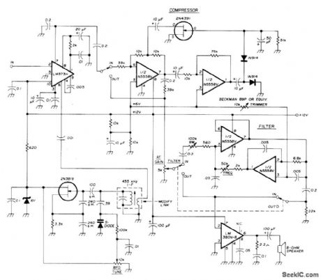
Combination of IF amplifier, audio compressor, tunable audio filter, and audio output system operates from single supply. Compressor and filter each use N5558V dual opamps or equivalent units. Tuning range of filter is about 500 to 2000 Hz. IF input goes directly to pin 2 of LM373H.Use coupling capacitor to prevent shorting pin 2 to ground and damaging IC.-R. Megirian, Design ldeasfor Miniature Communications Receivers, Ham Radio, April 1976, p 18-25. (View)
View full Circuit Diagram | Comments | Reading(792)
LOW_NOISE_FET_PREAMPLIFIER
Published:2009/7/21 6:21:00 Author:Jessie
For 600-ohm source, 3-db response is 0.5 cps to 700 kc, with voltage gain of 10.5, using common-emitter direct-coupled amplifier stage after fet stage, with 26 db of feedback. With 1-meg source, upper limit is 20 kc.-E. G. Fleenor, Low-Noise Preamplifier Uses Field-Effect Transistors, Electronics, 36:15, p 67-69. (View)
View full Circuit Diagram | Comments | Reading(1456)
10_CPS_TO_100_KG_BANDPASS
Published:2009/7/21 6:20:00 Author:Jessie

Input impedance is over 1 meg. Can be used in microphone case to raise power level of signal above that of interference. Both positive and negative feedback are used. Q1 and Q3 are 2N1086A, and Q2 is 2N414.-J. J. Tiemann, Transistor Amplifier with Adjustable Impedance and Gain, Electronics, 35:15, p 68-69. (View)
View full Circuit Diagram | Comments | Reading(631)
AUTOMATIC_INPUT_IMPEDANCE_MATCHER
Published:2009/7/21 6:18:00 Author:Jessie
Uses controlled amounts of negative feedback to maintain practically constant voltage sensitivity for impedances from 10 ohms to over 10,000 ohms.-Preamp Matches Input Impedance, Electronics, 31:13, p 81. (View)
View full Circuit Diagram | Comments | Reading(564)
| Pages:107/250 At 20101102103104105106107108109110111112113114115116117118119120Under 20 |
Circuit Categories
power supply circuit
Amplifier Circuit
Basic Circuit
LED and Light Circuit
Sensor Circuit
Signal Processing
Electrical Equipment Circuit
Control Circuit
Remote Control Circuit
A/D-D/A Converter Circuit
Audio Circuit
Measuring and Test Circuit
Communication Circuit
Computer-Related Circuit
555 Circuit
Automotive Circuit
Repairing Circuit