
Amplifier Circuit
Index 114
3_W_PULSE_AMPLIFIER
Published:2009/7/6 6:43:00 Author:May
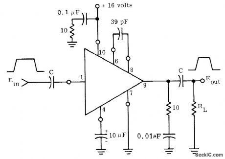
Motorola MC1554 power amplifier provides voltage gain of 18 for peak pulse power output up to 3 W Maximum peak output current rating of 500 mA for IC should not be exceeded during peak of output pulse.- The MC1554 One-Watt Monolithic Integrated Circuit Power Amplifier, Motorola, Phoenix, AZ, 1972, AN-401, p 3. (View)
View full Circuit Diagram | Comments | Reading(858)
POSTAMPLIFIER
Published:2009/7/6 6:35:00 Author:May

CMOS transistor pall fromCA3600E transistor array provides additional 30-dB gain above 100-dB gain of CA3080 opamp to give total of 130 dB. Current output is about10 mA. Remaining transistor pairs of array can be paralleled pail shown to give greater output. – Linear Integrated Circuits and MOS/FET's, RCA Solid State Division, Somerville, NJ, 1977, p 278-279. (View)
View full Circuit Diagram | Comments | Reading(715)
POWER_OPAMP
Published:2009/7/6 6:23:00 Author:May

Transistor Q1 and power transistor IC Q2 form equivalent of power PNP transistor for use with NPN LM195 power transistor IC serving as output stage for opamp. Circuit is stable for almost any load. Bandwidth can be increased to 150 kHz with full output response by decreasing C1 to 15 pF if there is no capacitive load to cause oscillation.- Linear Applications, Vol. 2, National Semiconductor, Santa Clara, CA, 1976, AN-110, p 5-6. (View)
View full Circuit Diagram | Comments | Reading(880)
Precision_absolute_value_circuit
Published:2009/7/22 22:43:00 Author:Jessie
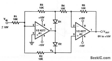
The values and types for D1 and D2 are not critical, but both diodes should be the same, and both must be able to withstand ±15 V (such as a 1N914). (View)
View full Circuit Diagram | Comments | Reading(0)
High_stability_thermocouple_amplifier
Published:2009/7/22 22:40:00 Author:Jessie
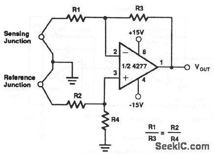
Notice that the reference-junction output is applied to the noninverting input of the 4277, and the sensing-junction output is applied to the inverting input. (View)
View full Circuit Diagram | Comments | Reading(0)
Lighting (Contd.) and Brake Lights Circuit Principle Diagram of Liberation CA6440 Series Light Buses
Published:2011/7/20 0:39:00 Author:Michel | Keyword: Liberation, Light Buses, Lighting, Brake Lights Circuit, Principle Diagram
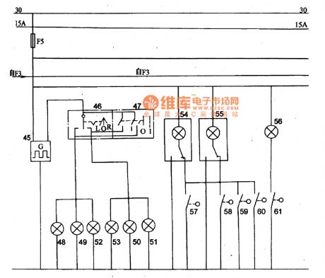
Picture:Lighting (contd.) and Brake Lights Circuit Principle Diagram of CA6440 Series Light Buses
45-flasher,46- turn signal swich,47-danger alertion switch,48 to 51一left and right direction indicator tell-tale,52 and 53-left and right indicator,54 and 55- indoor lamp,56- courtesy lamp,57-61-gate controlled switch. (View)
View full Circuit Diagram | Comments | Reading(587)
5_W_POWER_OPAMP
Published:2009/7/6 5:56:00 Author:May

Low-cost phono amplifier using only single 591 power opamp provides 5 W into 8-ohm load with only 0.2% total harmonic distortion. With crystal cartridge, circuit has fixed gain of 50.-R. J. Apfel, Power Op Amps-Their Innovative Circuits and Packaging Provide Designers with More Options, EDN Magazine, Sept. 5, 1977, p 141-144. (View)
View full Circuit Diagram | Comments | Reading(966)
RIAA_PHONO_PREAMP
Published:2009/7/6 5:56:00 Author:May

Design procedure is given for operation from 30-V supply, using magnetic cartridge having 0.5 mV/cm/s sensitivity. Will drive power amplifier having 5 VRMS input overload limit.-“Audio Handbook,”National Semiconductor, Santa Clara, GA, 1977, p 2-25-2-31. (View)
View full Circuit Diagram | Comments | Reading(1774)
MAGNETIC_PICKUP_PREAMP_1
Published:2009/7/6 5:55:00 Author:May

JFET input provides proper loading for variable-reluctance magnetic phono cartridge Gain of preamp is about 35 dB at 1 kHz (100-mV output for 2.2-mV input). Dynamic range is 84 dB referenced to 1 kHz Circuit includes feedback for RIAA equalization.-“FET Databook,” National Semiconductor, Santa Clara, CA, 1977, p 6-26-6-36. (View)
View full Circuit Diagram | Comments | Reading(2493)
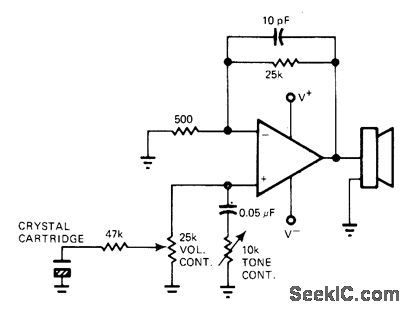
CERAMIC_CARTRIDGE_AMPLIFIER
Published:2009/7/6 5:54:00 Author:May
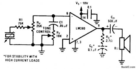
Single National LM380 forms simple amplifier with tone and volume controls for driving 8-ohm loud-speaker at outputs above 3 W. Supply voltage range is 12-22 V, with higher voltage giving higher power. Tone control changes high-frequency rolloff.- Audio Handbook, National Semiconductor, Santa Clara, CA, 1977, p 4-21-4-28. (View)
View full Circuit Diagram | Comments | Reading(1517)
LOW_NOISE_PREAMP
Published:2009/7/6 5:53:00 Author:May
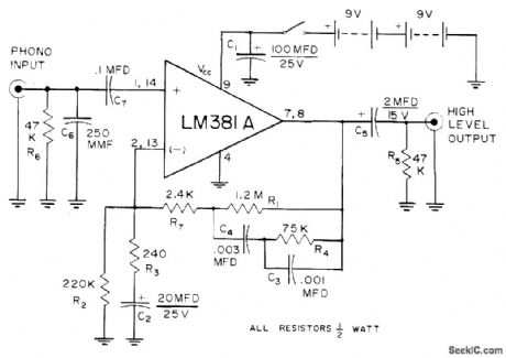
Provides dynamic range of about 80 dB for phonograph playback system, even when using highest-quality cartridge having low output. Source voltage is reduced to 18 V for National LM381A, which still provides ample signal for 2-V high-level input of stereo channel. Cross-channel isolation is better than 60 dB from 20 to 20,000 Hz.-J. P. Holm, A Quiet Phonograph Preamplifier, Audio, Oct. 1972, p 34-35. (View)
View full Circuit Diagram | Comments | Reading(896)
MAGNETIC_PICKUP_PREAMP
Published:2009/7/6 5:50:00 Author:May
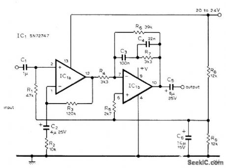
Circuit uses type 747 dual opamp, but individual 741 opamps may be used instead. Input signal is first amplified flat, after which equalization acts on both signal and noise to give improved S/N ratio. Adjust first opamp for gain of 13. Series feedback is used to minimize noise since impedance of magnetic pickup is low compared to opamp input impedance. Second opamp has frequency-dependent series feedback for RIAA compensation. Gain here is unity at 1 kHz. Out-put is about 70 mV for modern pickup having output of about 5 mV.-B. S. Wolfenden, Magnetic Pick-Up Preamplifier, Wireless World, Sept. 1976, p 81-82. (View)
View full Circuit Diagram | Comments | Reading(1806)
12_V_PHONO_PREAMP
Published:2009/7/6 5:47:00 Author:May

Low-noise circuit has midband 0-dB reference gain of 46 dB. Designed for RIAA response. Internal resistor matrix of IC minimizes parts count. Input is from magnetic cartridge.- Audio Handbook, National Semi-conductor, Santa Clara, CA, 1977, p 2-25-2-31. (View)
View full Circuit Diagram | Comments | Reading(628)
Three_op_amp_instrumentation_amplifier
Published:2009/7/23 21:11:00 Author:Jessie

This circuit uses only OP-37 ICs for instrumentation applications, whore low noise, wide bandwidth, low input-offset TC, and low input-bias currents are required.
(View)
View full Circuit Diagram | Comments | Reading(724)
High_speed_low_VSUBOS_SUB_composite_amplifter
Published:2009/7/23 20:36:00 Author:Jessie
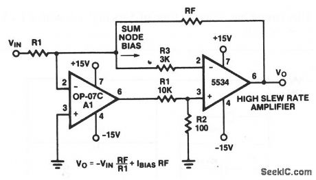
This circuit combines an OP-07C and a 5534 to form a high-speed amplifier with low output offset voltage. Notice that VO depends primarily on RF and R1. (View)
View full Circuit Diagram | Comments | Reading(1126)
OVERVOLTAGE_PROTECTOR
Published:2009/7/6 5:22:00 Author:May
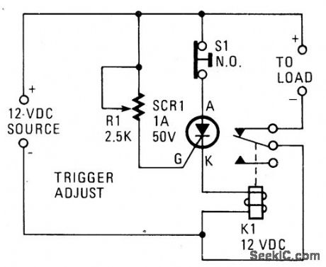
A silicon-controlled rectifier is installed in parallel with the 12-V line and connected to a normally-closed 12-V relay, K1. The SCR's gate circuit is used to sample the applied voltage. As long as the applied voltage stays below a given value, SCR1 remains off and K1's contacts remain closed, thereby supplying power to the load. When the source voltage rises above 12 V, sufficient current is applied to the gate of SCR1 to trigger it into conduction. The trigger point of SCR1 is dependent on the setting of R1. Once SCR1 is triggered (activating the relay), K1's contacts open, halting current flow to the load. (View)
View full Circuit Diagram | Comments | Reading(608)
2_METER_POWER_AMPLIFIER
Published:2009/7/6 5:09:00 Author:May


Provides 10-dB gain with full 30-W output at 160MHz and about 0.5-dB more gain at 150 MHz, using Motorola MRF238 transistor. C1-C4 are Arco 463, 464 or 424. RFC1 is 10 turns No. 20 on 270-ohm 1/2-W resistor. C5 is three 90-pF silver mica in parallel.RFC2 is 6 to 8 turns No. 18on toroid. L1 is 1/2turn No. 141 1/2inch long. L2 is 4 turns No. 14 spaced on 1/4inch diameter. L3 is 1 1/4-inch curve of No.14. D1-D8 are 1N4148. T1 and T2 are one quarter-wavelength of RG-174 or similar 50-ohm coax. D9 is 2-A silicon rectifier.-D. J.Lynch, Build a 2m Power Amp, 73 Magazine, Nov. 1977, p 96-97. (View)
View full Circuit Diagram | Comments | Reading(2202)
A_10_WATT_225_400_MHz_AMPLIFIER
Published:2009/7/6 5:06:00 Author:May

Circuit Notes
This broadband amplifier covers the 225-400 MHz military communications band producing 10 watt RF output power and operating from a 28 volt supply. The amplifier can be used as a driver for higher power devices such as 2N6439 and MRF327. The circuit is designed to be driven by a 50 ohm source and operate into a nominal 50 ohm load. The input matching network consists of a section composed of C3, C4, Z2, C5 and C6. C2 is a dc blocking capacitor, and T1 is a 4:1 impedance ratio coaxial transformer.Z1 is a 50 ohm transmission line. A compensation network consisting of R1, C1, and L1 is used to improve the input VSWR and flatten the gain response of the amplifier.L2 and a small ferrite bead make up the base bias choke. The output network is made up of a microstrip L-section consisting of Z3 and C7, and a high pass section consisting of C8 and L3. C8 also serves as a dc blocking capacitor. Collector decoupling is accom-plished through the use of L4, L5, C9, C10, C11, C12, and C13. (View)
View full Circuit Diagram | Comments | Reading(1376)
IMPROVED_RF_ISOLATION_AMPLIFIER
Published:2009/7/6 5:03:00 Author:May

Circuit Notes
This wideband RF isolation amplifier has a frequency response of 0.5 to 400MHz±0.5dB. This two stage amplifier can be used in applications requiring high reverse isolation, such as receiver intermediate-frequency (IF) strips and frequency distribution systems. Both stages use complementary-symmetry transistor arrangements. The input stage is a common-base connection for the complementary circuit. The output stage, which supplies the positive gain, is a common-emitter circuit using emitter degeneration and collector-base feedback for impedance control. (View)
View full Circuit Diagram | Comments | Reading(1805)
BROADCAST_BAND_PF_AMPLIFIER
Published:2009/7/6 4:59:00 Author:May

Circuit Notes
The circuit has a frequency response ranging from 100 Hz to 3 MHz; gain is about 30 dB. Field-effect transistor Q1 is configured in the common-source self-biased mode; optional resistor R1 sets the input impedance to any desired value. Commonly, it will be 50 ohms. The signal is then direct-coupled to Q2, a common-base circuit that isolates the input and output stages and provides the amplifier's exceptional stability. Q3 functions as an emitter follower, to provide low output impedance (about 50 ohms). For higher output impedance, include resistor R8. It will affect impedance according to this formula: R8~Rout-50. Otherwise, connect output capacitor C4 directly to the emitter of Q3. (View)
View full Circuit Diagram | Comments | Reading(769)
| Pages:114/250 At 20101102103104105106107108109110111112113114115116117118119120Under 20 |
Circuit Categories
power supply circuit
Amplifier Circuit
Basic Circuit
LED and Light Circuit
Sensor Circuit
Signal Processing
Electrical Equipment Circuit
Control Circuit
Remote Control Circuit
A/D-D/A Converter Circuit
Audio Circuit
Measuring and Test Circuit
Communication Circuit
Computer-Related Circuit
555 Circuit
Automotive Circuit
Repairing Circuit