
Amplifier Circuit
Index 113
LOW_FLOW_RATE_THERMAL_FLOWMETER
Published:2009/7/6 9:10:00 Author:May
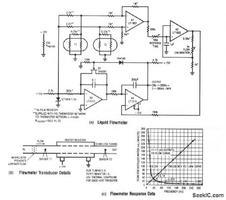
This design measures the differential temperature between two sensors. Sensor T1, located before the heater resistor, assumes the fluid's temperature before it is heated by the resistor. Sensor T2 picks up the temperature rise induced into the fluid by the resistor's heating. The sensor's difference signal appears at A1's output. A2 amplifies this difference with a time constant set by the 10 MΩ adjustment. Fig. 33-1c shows A2's output versus flow rate. The function has an inverse relationship. A3 and A4 linearize this relationship, while simultaneously providing a frequency output. A3 functions as an integrator that is biased from the LT1004 and the 338-KΩ input resistor. Its output is compared to A2's output at A4. Large inputs from A2 force the integrator to run for a long time before A4 can increase, tuming on Q1 and reset-ting A3. For small inputs from A2, A3 does not have to integrate long before resetting action occurs. Thus, the configuration oscillates at a frequency which is inversely proportional to A2's output voltage. Since this voltage is inversely related to flow rate, the oscillation frequency linearly corresponds to flow rate. (View)
View full Circuit Diagram | Comments | Reading(810)
PT2399 Digital Reverb Processing Integrated Circuit
Published:2011/7/23 4:44:00 Author:Michel | Keyword: Digital Reverb, Integrated Circuit


PT2399 is one typical karaoke echo processing integrated circuit which is widely used in CD, VCD, DVD, TV sound and karaoke.
First,PT2399 Inside Circuit Block Diagram and Pins Functions
There are A/D and D/A converter within PT2399 IC.And the input analog voice signal needs digital processing.Its inside circuit block diagram of the intergrated block is shown s picture 1.And the pins functions of the IC is shown as table 1.
Table 1:Pins Functions of PT2399 IC
Second,PT2399 Typical Application Circuit
According to PT2399 internal and external resistance connection,its typical equivalent circuit is shown as picture 2.
(View)
View full Circuit Diagram | Comments | Reading(9541)
BRIDGE_TRANSDUCER_AMPLIFIER
Published:2009/7/6 8:50:00 Author:May
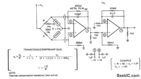
In applications involving strain gauges, accelerometers, and thermal sensors, a bridge transducer is often used. Frequently, the sensor elements are high resistance units requiring equally high bridge resistance for good sensitivity. This type of circuit then demands an amplifier with high input impedance, low bias current and low drift. The circuit shown represents a possible solution to these general requirements. (View)
View full Circuit Diagram | Comments | Reading(0)
Multiplexed_video_amplifier
Published:2009/7/22 6:49:00 Author:Jessie

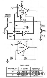

This circuit is a simple way to multiplex two video amplifiers onto a single 75-Ω cable. The appropriate amplifier is activated in accordance with the truth table. Amplifier performance includes 0.02% differential gain error and 0.1' differential phase error. The 75-Ω back termination (looking into the cable) means that the amplifier must swing 2 Vpp to produce 1 Vpp at the cable output. (View)
View full Circuit Diagram | Comments | Reading(594)
Counter Circuit of SN7490
Published:2011/7/24 8:37:00 Author:Michel | Keyword: Counter Circuit
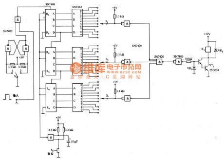
Picture 1 is counter circuit of SN7490.It is accumulating counting circuit of the pulse added to A port.Usually,it is used in counting of input pulse.S4一S6 are reset switches used in counting setting.The corresponding relay controls relative circuit action.If the time pulse shown as picture 1 is connected to A terminal and it can also constitute digital timing circuit which uses power supply frequency as benchmark.
Picture 1:Counter Circuit of SN7490 (View)
View full Circuit Diagram | Comments | Reading(2055)
400_VDC_SWITCH
Published:2009/7/6 7:40:00 Author:May
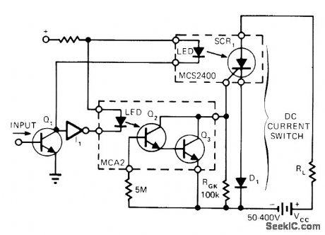
Optically isolated photo-SCR serves for switching high-voltage DC. Turnoff of SCR occurs when Q3 in MCA2 photo-Darlington shunts load current through gate, bypassing gate-cathode junction within SCR. Circuit can be operated by pulsing appropriate LEDs to turn SCR on or off. Without input signal, inverter maintains current through LED of MCA2 to keep SCR clamped off.-G. C. Riddle, Opto-Isolators Switch High-Voltage DC Cur-rent, EDN Magazine, Feb. 5, 1975, p 54. (View)
View full Circuit Diagram | Comments | Reading(1180)
TWO_MHz_SQUARE_WAVE_GENERATOR_USES_TWO_TTL_GATES
Published:2009/7/6 7:26:00 Author:May
With the values shown the circuit generates a 2-MHz symmetrical square wave. Changing capacitors C1 and C2 to 0.01 μF results in a frequency of 500 Hz. For the particular integrated circuits and power supply voltages (5.0 V), the reliable operating range of R1 = R2 is 2 k ohm to 4 k ohm. (View)
View full Circuit Diagram | Comments | Reading(742)
PULSE_AMPLIFIER
Published:2009/7/6 7:15:00 Author:May
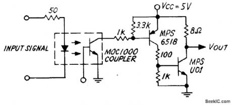
Motorola MOC1000 optoisolator permits coupling digital logic to system having different supply voltages or unequal grounds while providing essentially complete isolation. Circuit provides transfer characteristics needed in instrumentation applications and has sufficient drive for handling low input impedances.- Industrial Control Engineering Bulletin, Motorola, Phoenix, AZ, 1973, EB-4. (View)
View full Circuit Diagram | Comments | Reading(1040)
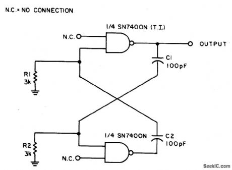
COMPLEMENTARY_POSTAMPLIFIER
Published:2009/7/6 7:10:00 Author:May
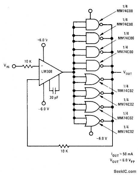
Paralleled NAND gates provide buffering for LM308 opamp while increasing current drive to about 50 mA for 6 V P-P output,MM74C00 NAND gates supply about 10 mA each from positive supply while MM74C02 gates supply same amount from negative supply.- Linear Applications, Vol. 2, National Semiconductor, Santa Clara, GA, 1976, AN-88, p 2-3. (View)
View full Circuit Diagram | Comments | Reading(611)
STEAM_TRAIN_PROP_PLANE
Published:2009/7/6 7:08:00 Author:May
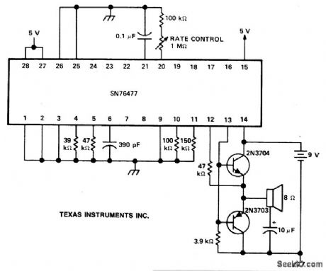
View full Circuit Diagram | Comments | Reading(892)
SUMMING_OPAMP
Published:2009/7/6 7:04:00 Author:May
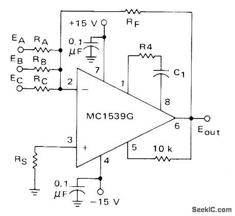
Motorola MC1539 serves as closed-loop summing amplifier having very small loop-gain error because of high open-loop gain. RS should equal parallel combination of RA, RB, RC, and RF.-E. Renschler, The MC1539 Operational Amplifier and Its Applications, Motorola, Phoenix, AZ, 1974, AN-439, p 18. (View)
View full Circuit Diagram | Comments | Reading(800)
300_Hz_VOLTAGE_FOLLOWER
Published:2009/7/6 7:03:00 Author:May
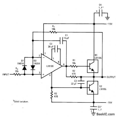
Simpie LM195 power output stage provides 1-A output for voltage-follower connection of LM108 opamp.-R. Dobkin, Fast IC Power Transistor with Thermal Protection, National Semiconductor, Santa Clara, CA, 1974, AN-110, p 6. (View)
View full Circuit Diagram | Comments | Reading(715)
GAIN_CONTROLLED_AMPLIFIER
Published:2009/7/6 6:55:00 Author:May
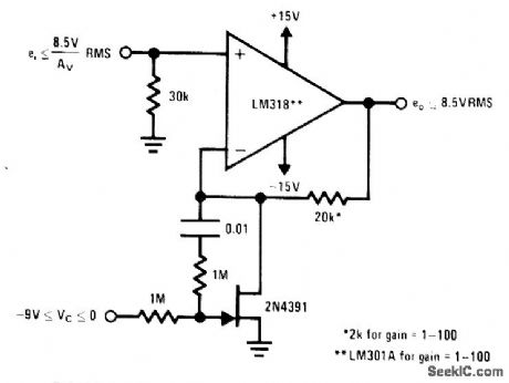
Control voltage in range of 0 to -9 V provides gain range of 1 to 1000 for National LM318 opamp using FET in feedback path. Bandwidth is better than 20 kHz at maximum gain. Applications include remote or multichannel gain control, volume expansion, and volume compression/limiting.-J. Sherwin, A Linear Multiple Gain-Controlled Amplifier, National Semiconductor, Santa Clara, CA, 1975, AN-129, p 5. (View)
View full Circuit Diagram | Comments | Reading(3959)
SINGLE_SUPPLY_POSTAMPLIFIER
Published:2009/7/6 6:51:00 Author:May
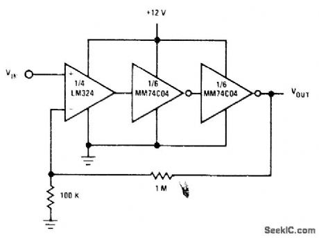
Use of two sections of MM74C04 as postamolifier for LM324 single-supply amplifier gives open-loop gain of about 160 dB Additional CMOS inverter sections can be paralleled for increased power to drive higher current loads; each MM74C04 section is rated for 5-mA load.- Linear Application, Vol. 2, National Semiconductor, Santa Clara, CA, 1976, AN-88, p 2. (View)
View full Circuit Diagram | Comments | Reading(765)
Optocoupler_that_is_used_as_a_pulse_amplifier
Published:2009/7/22 22:23:00 Author:Jessie
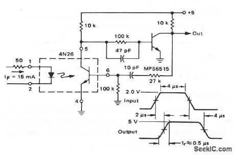
This circuit shows a 4N26 combined with a transistor to form a simple pulse amplifier that uses positive feedback to the 4N26 base. The feedback decreases pulse rise time from about 2 to 0.5 μs. (View)
View full Circuit Diagram | Comments | Reading(864)
P87C766 Single-chip Microcomputer Integrated Circuit
Published:2011/7/28 22:12:00 Author:Michel | Keyword: Single-chip, Microcomputer, Integrated Circuit
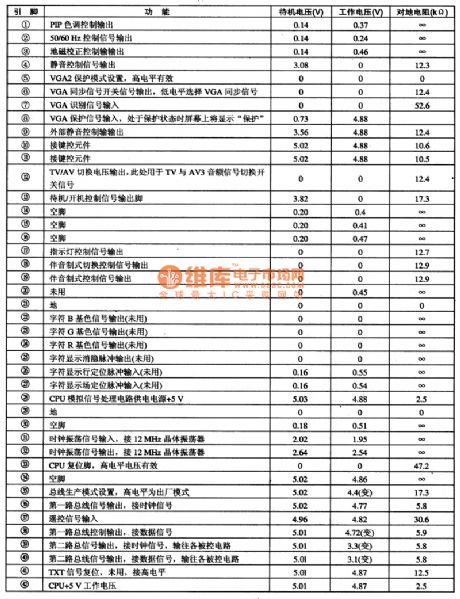
P87C766 is single-chip microcomputer integrated circuit produced by Phlips Company and it is special main control chip of ChangHong DT2000 frequency doubling color TV electric set.
First,Function Features P87C766 contains the CPU (central processing unit), the I2C bus circuit, OSD showing circuit, all kinds of identification signal circuit, all sorts of function control circuit, and some other auxiliary functions circuit.
Second,Pins Functions and Data
P87C766 IC adopts feet 42 DI{ package and P87C766 on DT2000 color TV and its pins functions and data are shown as table 1.The voltage of the table, change means that it is in unstable condition when the voltage is measured.
(View)
View full Circuit Diagram | Comments | Reading(586)
Optically_coupled_RS_flip_flop
Published:2009/7/22 22:16:00 Author:Jessie
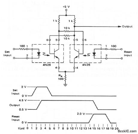
This circuit uses two 4N26 couplers to form an RS circuit with two stable states. A +2-V signal at the set input changes the output from low to high, and a +2-V signal at the reset input returns the output to low. The input pulse width must be 3 μs (minimum). (View)
View full Circuit Diagram | Comments | Reading(885)
RESISTANCE_CHECKER
Published:2009/7/22 22:15:00 Author:Jessie
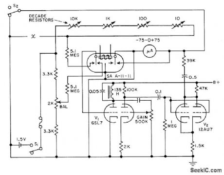
Amplified error voltage from Wheatstone bridge feeds 75-0-75 microammeter to indicate whether resistance under test is higher or lower than desired value und within preset tolerance. Instrument range is 9,999 ohms in 1-ohm steps. Gives go-no-go indication, to speed production testing.-D. S. Randall, Go No-Go Meter Speeds Resistance Check, Electronics, 31;9, p 66-68. (View)
View full Circuit Diagram | Comments | Reading(740)
FEED_FORWARD_OPAMP
Published:2009/7/6 6:51:00 Author:May
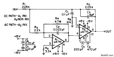
DC input characteristics are determined by A1, which is bypassed at high frequencies, while AC-coupled A2 deter-mines dynamic performance. Resulting composite amplifier combines such desired properties as low input current and drift, large bandwidth and slew rate, and fast settling time. Compensation network C3-C4-C5 is chosen first to give desired bandwidth. Composite rolloff of 6 dB per octave is then obtained by narrow-banding A1 with R4 and C2, so gain-bandwidth product is equal to ratio between unity-gain crossover frequency of A2 and open-loop gain.-Fairchild Linear IC Contest Winners, EEE Magazine, Jan. 1971, p 48-49. (View)
View full Circuit Diagram | Comments | Reading(915)
SUMMING_WITHOUT_ADJUSTMENTS
Published:2009/7/6 6:44:00 Author:May
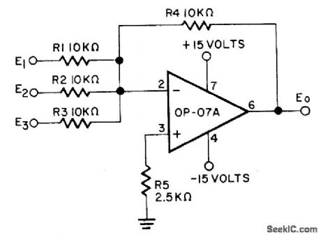
Single-stage opamp for analog computation provides high-precision output that is function of multiple input variables. Circuit drift is less than 2μV per month, eliminating need for periodic calibration while ensuring long-term accuracy. Opamp is Precision Monolithics op-07A.-D. Soderquist and G. Erdi, The op-07 Ultra-Low Offset voltage op Amp-a Bipolar Op Amp. That Challenges Choppers, Eliminates Nulling, Precision Monolithics, Santa Clara, CA, 1975, AN-13, p 11. (View)
View full Circuit Diagram | Comments | Reading(769)
| Pages:113/250 At 20101102103104105106107108109110111112113114115116117118119120Under 20 |
Circuit Categories
power supply circuit
Amplifier Circuit
Basic Circuit
LED and Light Circuit
Sensor Circuit
Signal Processing
Electrical Equipment Circuit
Control Circuit
Remote Control Circuit
A/D-D/A Converter Circuit
Audio Circuit
Measuring and Test Circuit
Communication Circuit
Computer-Related Circuit
555 Circuit
Automotive Circuit
Repairing Circuit