
Amplifier Circuit
Index 104
SIDEBAND_RF_AMPLIFIER
Published:2009/7/9 1:02:00 Author:May

This RF amplifier has wide bandwidth and dynamic range. It has a gain of 10 dB, noise figure less than 5 dB, and the third-order 1 MD is -40 dB at +22 dBm/tone output. The bandwidth is 4 to 55 MHz. (View)
View full Circuit Diagram | Comments | Reading(795)
1500_W_BF_AMPLIFIER
Published:2009/7/9 1:01:00 Author:May
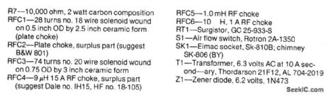
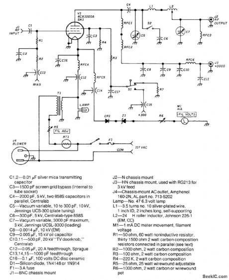
The frequency range of this amplifier is 1.8 to 54 MHz.The amount of RF drive required for full out-put is about 30 W. The grid compartment (R1, R2, RFC4,RFC5)should be shielded from the othercircuitry-especially the output circuitry. (View)
View full Circuit Diagram | Comments | Reading(583)
4_W_AMPLIFIER_FOR_900_MHz
Published:2009/7/9 0:56:00 Author:May
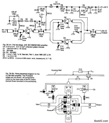
Using Wilkinson power dividers in the base and collector circuits of Q2 and Q3, two SD1853 devices are paralleled for twice the power output of the 2-W amplifier. (View)
View full Circuit Diagram | Comments | Reading(683)
7__10__15__20__25__35_watt_AF_power_amplifier_with_PNP_driver
Published:2009/7/20 21:32:00 Author:Jessie
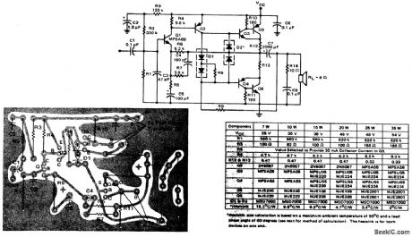
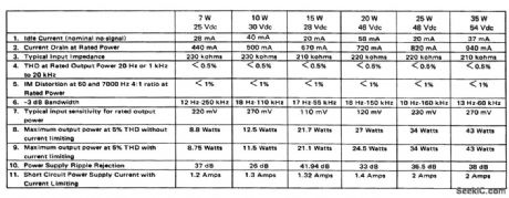
7-/10-/15-/20-/25-/35-watt AF power amplifier with PNP driver (courtesy Motorola Semiconductor Products Inc.). (View)
View full Circuit Diagram | Comments | Reading(796)
VIDEO_OUTPUT_AMP
Published:2009/7/20 21:04:00 Author:Jessie
With 2N834 circuit, output is sufficient to drive crt.-W. D, Roehr, Epitaxial Process Improves Transistor Charateristics, Electronics, 34:9, p 52-53. (View)
View full Circuit Diagram | Comments | Reading(599)
15__20__25__35__50__60_watt_AF_power_amplifier_with_DC_coupled_output
Published:2009/7/20 20:58:00 Author:Jessie
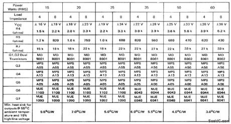
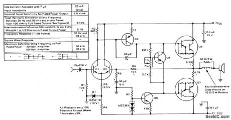
15-/20-/25-/35-/50-/60-watt AF power amplifier with DC-coupled output (courtesy Motorola Semiconductor Products Inc.). (View)
View full Circuit Diagram | Comments | Reading(1642)
+12_V_SERIES_EMITTER_FOLLOWER
Published:2009/7/8 23:38:00 Author:May

Baseemitter voltageis more orless constant withoutuse offeedback because baseis held at constant voltage by zener diode Ripple at base is reduced by RC filter.-H,Olson Power-Supply Servicing Ham Radio, Nov 1976、p44-50 (View)
View full Circuit Diagram | Comments | Reading(828)
VIDEO_DISTRIBUTION_AMPLIFIER
Published:2009/7/20 20:56:00 Author:Jessie

Bandwidth is 12 Mc, for high-resolution closed-circuit television and high-speed facsimile systems. Input level is 2 v and output level is 5 v for 75.ohm lines. Differential amplifier eliminates second harmonic distortion without use of interstage transformers.-H. H. Naidich, Video Distribution Amplifier Eliminates Interstage Transformers, Eectronics, 34:24, p 58-61.
(View)
View full Circuit Diagram | Comments | Reading(0)
CASCODE_RF_AMPLIFIER
Published:2009/7/9 1:23:00 Author:May
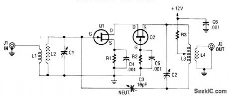
A cascode amplifier using two MOSFETs is shown in the diagram. L2C1 and L3C2 resonate to the frequency in use. The circuit has the advantage of good gain, low NF, and excellent linearity. Q1 and Q2 can be MPF102 or 2N4416. (View)
View full Circuit Diagram | Comments | Reading(2036)
VIDEO_LINE_DRIVING_AMPLIFIER
Published:2009/7/9 1:22:00 Author:May

Q1 and Q2 form a differential stage which single-ends into the LT1010. The capacitively terminated feedback divider gives the circuit a dc gain of 1, while allowing ac gains up to 10. Using a 20-Ω bias resistor, the circuit delivers 1 V pk-pk into a typical 75-Ω video load. For applications sensitive to NTSC requirements, dropping the bias resistor value will aid performance. At A = 2, the gain is within 0.5 dB to 10 MHz and the -3 dB point occurs at 16 MHz. At A = 10, the gain is flat, with ±0.5 dB to 4 MHz .and the -3 db point occurs at 8 MHz。The peaking adjustment should be optimized under loaded output conditions. (View)
View full Circuit Diagram | Comments | Reading(1034)
1296_MHz_RF_AMPLIFIER
Published:2009/7/9 1:16:00 Author:May
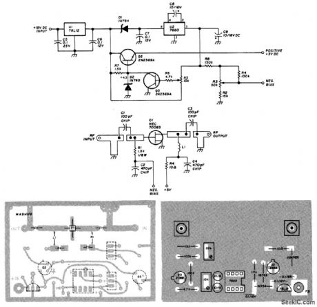
Using an NEC70083, this 1296-MHz amplifier delivers about 17-dB gain and around 1- to 1.5-dB noise. It is constructed on a G-10 epoxy fiberglass PC board. Use the layout shown because this is impor-tant for correct performance.The power supply/regulator delivers the regulated 3-Vdc for the drain circuit and U2 produces a nega-tive bias for the gate circuit. R5 sets the drain voltage to+3 V and R3 sets the gate bias. Typically, the drain current is about 10 mA. (View)
View full Circuit Diagram | Comments | Reading(1058)
LINE_OPERATED_AMPLIFIER
Published:2009/7/21 1:20:00 Author:Jessie
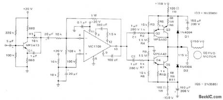
Push-pull phase shifter. single-ended preamp, and push-pull class B power amplifier all obtain supply voltages from AC supply that can either use power transformer or operate directly from line with diode rectifiers. Power output is enough to drive size 18 servomotor at 10W. Larger servomotors can be used if reduced supply voltages can be tolerated. Suitable power supply circuits are given.-A. Pshaenich, Servo Motor Drive Amplifiers, Motorola, Phoenix, AZ, 1972, AN-590. (View)
View full Circuit Diagram | Comments | Reading(0)
DC_GAIN_CONTROLLED_VIDEO_AMPLIFIE
Published:2009/7/9 1:32:00 Author:May
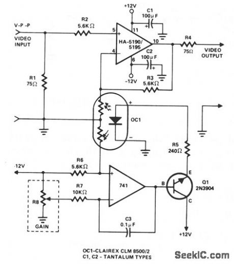
This amplifier employs a cascaded op amp inte-grator and transistor buffer, Q1, to drive the gain control element. Except for a simple modification, the HA-5190/5195 stage is connected as a conven-tional noninverting op amp, and includes input and output impedance matching resistors RI and R4, respectively, series stabilization resistor R2, and power supply bypass capacitors C1 and C2. The circuit differs from standard designs in that the gain control network includes a photoresistor, part of OC1. The optocoupler/isolator OC1 contains two matched photoresistors, both activated by a common LED. The effective resistances offered by these devices are inversely proportional to the light emitted by the LED. One photoresistor is part, with R3, of the HA-5190/5195 gain network, while the other forms a voltage-divider with R6 to control the bias applied to the integrator noninverting terminal.In operation, the dc voltage supplied by gain control R8 is applied to the integrator inverting input terminal through input resistor R7. Depending on the relative magnitude of the control voltage, the integrator output will either charge or discharge C3. This change in output, amplified by Q1, con-trols the current supplied to the OC1 LED through series limiting resistor R5. The action continues until the voltage applied to the integrator noninverting input by the R6-photoresistor gain network is changing, adjusting the op amp stage gain. As the control voltage at R8 is readjusted, the OC1 photoresistances track these changes, automatically readjusting the op amp in accordance with the new control voltage setting. (View)
View full Circuit Diagram | Comments | Reading(975)
Balance_differential_amplifier_with_a_controlled_constant
Published:2009/7/21 2:09:00 Author:Jessie

Balance differential amplifier with a controlled constant-current-souroe drive and AGC capability. Operation can be from DC to 120 MHz. Supply voltage is typically 9 to 12 volts (courtesy GTE Sylvania Incorporated). (View)
View full Circuit Diagram | Comments | Reading(530)
One_out_of_four_data_selector_using_MC1545G_wide_band_amplifiers
Published:2009/7/21 2:10:00 Author:Jessie
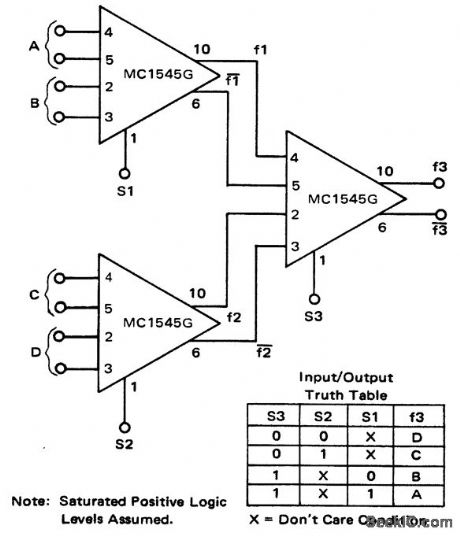
One-out-of-four data selector using MC1545G wide-band amplifiers. This circuit can be modified to be a one-out-of-N data selector (courtesy Motorola Semicon-ductor Products Inc.). (View)
View full Circuit Diagram | Comments | Reading(540)
VOLTAGE_CONTROLLED_AMPLIFIER
Published:2009/7/9 1:32:00 Author:May
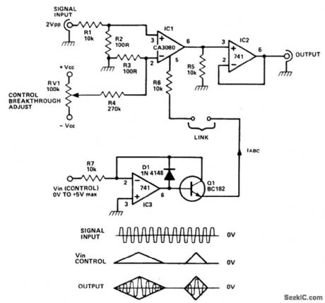
The CA3080 can be used as a gain controlling device. The input signal is attenuated by R1/R2 so that a 20-mVpp signal is applied to the input terminals. If this voltage is much larger, significant distortion will occur at the output. In fact, this distortion is put to good use in the triangle-to-sine wave converter.
The gain of the circuit is controlled by the magnitude of the current IABC. This current flows into the CA3080 at pin 5, which is held at one diode voltage drop above the - VCC rail. The gain of the CA3080 is linearly proportional to the magnitude of the IABC current over a range of 0.1μA to 1 mA. Thus, by controlling IABC, you can control the signal level at the output. The output is a current output, which has to be dumped into a resistive load (R5) to produce a voltage output. The output impedance at IC1 pin 6 is 10 kΩ (R5), but this is unloaded by the voltage follower (IC2) to produce a low output impedance.
The circuit around IC3 is a precision voltage-to-current converter and this can be used to generate IABC. When Vin (control) is positive, it linearly controls the gain of the circuit. When it is negative, IABC is zero and so the gain is zero. (View)
View full Circuit Diagram | Comments | Reading(0)
WIDEBAND_AMPLIFIER_1
Published:2009/7/9 1:31:00 Author:May

This wideband amplifier uses a MARI IC, which is a gain block. The device is manufactured by Mini-Circuits Lab and offers +13-dB gain from dc to 1000 MHz. R1 is selected to provide 17-mA current to UI at +5 V. For 12-V supply R1 = 470 Ω. RFC1 is typically 1 to 5 pH. (View)
View full Circuit Diagram | Comments | Reading(698)
BUFFER_AMPLIFIER_WITH_MODULATOR
Published:2009/7/9 1:28:00 Author:May
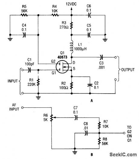
A 40673 MOSFET is used as a wideband buffer amplifter (to 20 MHz). If desired, the amplifier can be modulated, considering that the gate 2 voltage of a MOSFET can be used to vary the gain of the stage. (View)
View full Circuit Diagram | Comments | Reading(914)
WIDEBAND_AMPLIFIER
Published:2009/7/9 1:26:00 Author:May

Using a Signetics NE5205, this circuit gives about + 16-dB gain from LF to 600 MHz. The π mini-mizes load impedance and source-impedance variations and aids stability. (View)
View full Circuit Diagram | Comments | Reading(1922)
High-Voltage Isolating Current Detection Circuit (ISO212 And OPA27)
Published:2011/8/3 9:39:00 Author:Robert | Keyword: High-Voltage, Isolating, Current, Detection
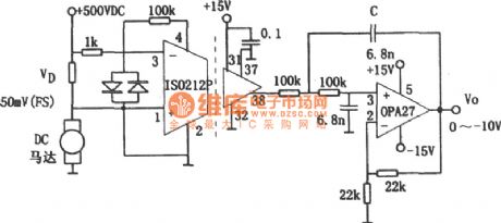
In the circuit which has hundreds of volts voltage, if you want to detect the current you must solve the voltage isolating problem. One kind of practical circuit that can meet the requirements above is shown in the picture. The circuit uses a isolating amplifier ISO212P. This element is dual-port isolating miniaturization IC. The motor shown in the picture is a DC motor with 500V power supply. It is added a little resistor in series with the motor's power supply loop circuit for current detection. The resistor's value's selection should satisfy that it could get the maximum voltage signal of 50mV at the maximum current. Because the signal got from the sampling resistor would be added into the isolating amplifier ISO212P's pin 3 by the the out-phase input method, the amplifier's in-phase input port (pin 1) would connect to the ground. It should be noted that the ISO212P's input ground (pin 2) and the motor's power supply's ground should be connected, which means they are not common in ground. (View)
View full Circuit Diagram | Comments | Reading(627)
| Pages:104/250 At 20101102103104105106107108109110111112113114115116117118119120Under 20 |
Circuit Categories
power supply circuit
Amplifier Circuit
Basic Circuit
LED and Light Circuit
Sensor Circuit
Signal Processing
Electrical Equipment Circuit
Control Circuit
Remote Control Circuit
A/D-D/A Converter Circuit
Audio Circuit
Measuring and Test Circuit
Communication Circuit
Computer-Related Circuit
555 Circuit
Automotive Circuit
Repairing Circuit