Amplifier Circuit
WIDEBAND_500_kHz_1_GHz_HYBRID_AMPLIFIER
Published:2009/7/7 7:57:00 Author:May | From:SeekIC

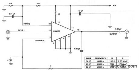
The amplifier's input stageis a dual-gate GaAs FET, which provides low mput capacitance and hightransconductance. The dual-gate structure accepts the signal on mput 1. Input 2 controls the gain of theamplifier. The amplifier has a third input for use h senes feedback. The output feeds back to pm 3 via asingle resistor, which controls the overall power galn of the ampllfter. At 10 MHz, the output is capable ofdelivering 12 dBm into a 50-Ω load with 1 dB of signal compression. The accoupled amplifier has a gam of 37 dB at 100 MHz and 3 dB at 1 GHz.
Reprinted Url Of This Article:
http://www.seekic.com/circuit_diagram/Amplifier_Circuit/WIDEBAND_500_kHz_1_GHz_HYBRID_AMPLIFIER.html
Print this Page | Comments | Reading(3)

Article Categories
power supply circuit
Amplifier Circuit
Basic Circuit
LED and Light Circuit
Sensor Circuit
Signal Processing
Electrical Equipment Circuit
Control Circuit
Remote Control Circuit
A/D-D/A Converter Circuit
Audio Circuit
Measuring and Test Circuit
Communication Circuit
Computer-Related Circuit
555 Circuit
Automotive Circuit
Repairing Circuit
Code: