Position: Home > Circuit Diagram > Amplifier Circuit > Large_signal_voltage_follower_with_000065_worst_case_accuracy_error
Amplifier Circuit
Large_signal_voltage_follower_with_000065_worst_case_accuracy_error
Published:2009/7/23 21:15:00 Author:Jessie | From:SeekIC
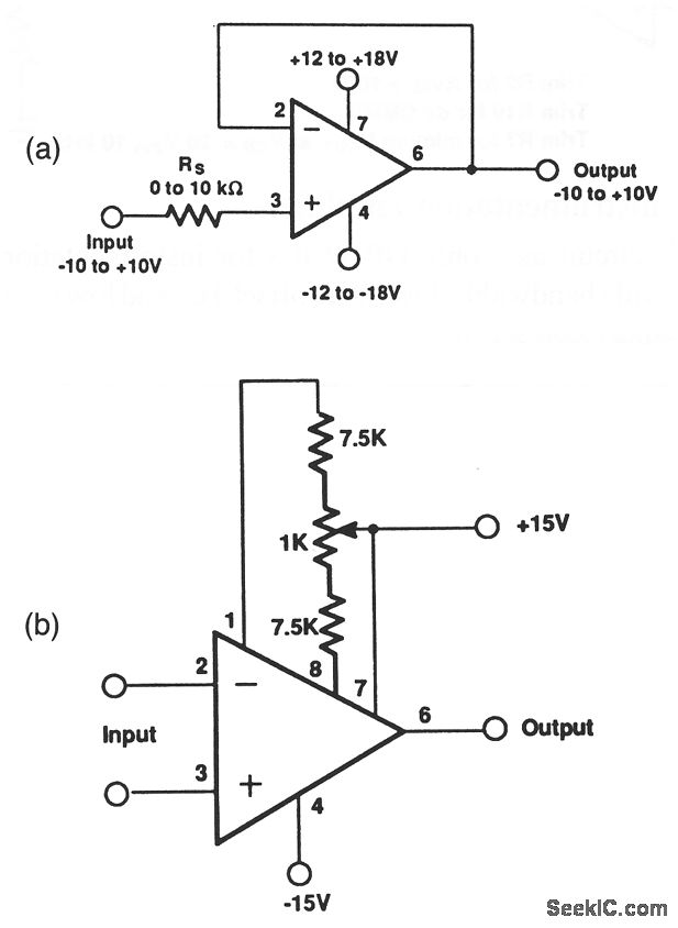
The input offset voltage and drift with temperature of the RC4097 that are shown in this voltage-follower circuit are trimmed at wafer test to a low level. However, if further adjustment of VOS is necessary, nulling with the circuit of Fig. 10-17B will not degrade drift with temperature. The Fig. 10-17B offset circuit has an approximate range of about 4 mV.
Reprinted Url Of This Article:
http://www.seekic.com/circuit_diagram/Amplifier_Circuit/Large_signal_voltage_follower_with_000065_worst_case_accuracy_error.html
Print this Page | Comments | Reading(3)

Article Categories
power supply circuit
Amplifier Circuit
Basic Circuit
LED and Light Circuit
Sensor Circuit
Signal Processing
Electrical Equipment Circuit
Control Circuit
Remote Control Circuit
A/D-D/A Converter Circuit
Audio Circuit
Measuring and Test Circuit
Communication Circuit
Computer-Related Circuit
555 Circuit
Automotive Circuit
Repairing Circuit
Code: