
Circuit Diagram
Index 830
LINE_OPERATED_SMOKE_DETECTOR
Published:2009/7/10 3:38:00 Author:May

Using an ionization chamber anda high-impedance (CA3130) op amp, the presence of smoke will cause the CA3130 to stop oscillating, triggering S106D SCR, sounding the alarm. (View)
View full Circuit Diagram | Comments | Reading(990)
DIGTAL_LED_VOLTMETER
Published:2009/7/10 3:37:00 Author:May

The voltage to be measured is digitized in an analog-to-digital (A/D) converter and then displayed in three decimal digits. The display consists of three groups of 10 LEDs. The meter can only be used for measuring direct voltages.
The A/D converter is based on CA3162, which can process direct voltage up to 999 mV (1-V full-scale deflection-FSD). The FSD is extended to 10 V with the aid of potential divider R1/R2/R3. Other ranges are possible by altering the values of the resistors.
The measured value is read from three bars of LEDs: the first one of these, D1 through D10, shows units; the second, D11 through D20 tens; and the third, D21 through D30, hundreds.
The circuit is nulled with P1 when the input is open. Zero here means that diodes D1 D11, and D21, light. Diodes D10, D20, and D30, represent the figure 9. Next, a known voltage is applied to the input and P2 is adjusted until the LEDs read the correct value. When the input voltage is too high, the display goes out. When the input is negative, the unit LEDs do not light. Notice that variations in the supply voltage affect the measurement adversely. (View)
View full Circuit Diagram | Comments | Reading(2545)
SCR_SLAVE_FLASH
Published:2009/7/10 3:37:00 Author:May

Using a light-activated SCR, this circuit can trigger a slave-flash unit. (View)
View full Circuit Diagram | Comments | Reading(845)
POWER_TO_VOLTAGE
Published:2009/7/10 3:36:00 Author:May

Two Oρamρs and inexpensiveIC multiplier provide output voltage directly ρroρortional to instantaneous power through load. Frequency response extends from DC to several kilohertz.Maximum load powerfor linearity is 2 kVA, with maximums of 400 V and 5 A for load voltage and current. Output voltage can vary from -10 V to +10 V depending on instantaneous polarities and magnitudes of load voltage and current. R1 determines current range, and R2 determines voltage range.-D. DeKold, Integrated Multiplier Simplifies Wattmoter Design, Electronics, Sept. 27, 1973, p 106-107; reprinted in Circuits for Electronics Engineers, Electronics, 1977, p 175-176. (View)
View full Circuit Diagram | Comments | Reading(626)
GAIN_CONTROLLED_AMPLIFIER
Published:2009/7/10 3:36:00 Author:May
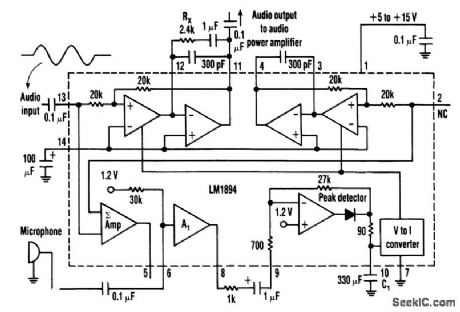
This single-chip circuit adjusts its audio gain according to the ambient nolse picked up by the mlcrophone。When operating in a quiet environment,the audio output is quiet,while a notsy environment resultsh a louder audio output。Audio to pm 13 is amplified by the variable-gain amplifier within the LM1894 IC,Audio from the microphone connected through 0.1μF capacitor to pin 6 controls the audio gain of thevariable-gam amplifier,The output appears on pm 11 andis taken off through an 0.1μ capacitor. (View)
View full Circuit Diagram | Comments | Reading(0)
CALIBRATED_TACHOMETER
Published:2009/7/10 3:36:00 Author:May

Here is a simple tachometer circuit for use with a hand-held DVM or portable chart recorder. A novel feature is that the source frequency pulse/rev rate can be directly set on a ten-turn potentiometer to provide a convenient calibration of one V per 1000 rev/min. This is particularly useful when measuring a shaft or engine speed by sensing gear teeth.The circuit uses an LM2917 IC which is specifically designed for tachometer applications. The ten-turn potentiometer, which provides the pulse/rev setting, is suitably conftgured in the output amplifter feedback path. The pulse/rev range is 100 to 1100, so the potentiometer dial mechanism should be set to start at 100 to provide direct calibration.The IC's internal 7.5-V zener provides stable operation from a 9-V battery. The tachometer accepts an input signal between 50 mv and 20 V rms and has an upper speed limit of 6000 rev/min with the compo-nent values shown. (View)
View full Circuit Diagram | Comments | Reading(2591)
TACHOMETER
Published:2009/7/10 3:34:00 Author:May

A standard shaft encoder's A and B ports generate square waves with the same frequency as the shaft turns. The phase of A will lead or lag that of B by 90°, depending on the direction of rotation. To obtain maximum resolution, the tachometer circuit must count every change of the state for the A and B signals. Each such change causes a change of state at IC1A's output, followed by a 1-μs negative pulse at the output of IC1C. These clock pulses' positive (trailing) edges cause the counter to count up or down, according to the direction of shaft rotation.You should set the R1C1 time constant, so that it is approximately twice that of the R2C2 product, to ensure adequate setup and hold times for the up/down signal with respect to the positive clock edges.IC1C supports this timing requirement by producing clock pulses of similar duration for either positive or negative transitions or IC1A.The exclusive-NOR logic of IC1B generates the correct polarity of the up/down signal when necessary, at the positive clock edges, by combining the A value with the B value just prior to a transition of A or B. C1 provides memory by sorting the B value voltage for about 2 μs. The maximum frequency for A or B is approximately (4R1C1)-1.
(View)
View full Circuit Diagram | Comments | Reading(0)
RF_FIELD_DETECTOR
Published:2009/7/10 3:34:00 Author:May

This detector is a half-wave rectifier for RF, which then feeds an op amp. U1A acts as an amplifier, driving meter M1. This circuit can detect mW RF levels from below the AM broadcast band to well above the FM broadcast band. (View)
View full Circuit Diagram | Comments | Reading(1580)
SSB_CW_PRODUCT_DETECTORS
Published:2009/7/10 3:33:00 Author:May

These circuits are used for product detection of single-sidebound (SSB) and CW signals. BFO injection is typically 0.5 to 1 V rms for both circuits. Frequencies can be up to 25 MHz or so. (View)
View full Circuit Diagram | Comments | Reading(1550)
SYNCHRONOUS_SYSTEM
Published:2009/7/10 3:32:00 Author:May


The circuit uses a synchronous-detection scheme to measure low-level resistances. Other low-resis-tance-measuring circuits sometimes inject unacceptable large currents into the system-under-test.This circuit synchronously demodulates the voltage drop across the system-under-test and can hence use extremely low currents while measuring resistance.The 10-V (pk), 1-kHz carrier generator injects a 1-mA reference current into unknown resistor, RTEST. Instrument amplifier IC1 and precision op amp IC2A amplify the voltage across RTEST by a gain of 100000. Synchronous detector IC3 demodulates this voltage, then op amp IC2B acts a low-pass filter on the demodulated voltage. The low-pass filtering will attenuate all uncorrelated disturbances (such as noise, drift, or offsets), while passing a dc voltage that is proportional to the unknown resistance.
The relationship between the output voltage and the unknown resistance is:
(View)
View full Circuit Diagram | Comments | Reading(836)
PHOTO_EVENT_TIMER
Published:2009/7/10 3:32:00 Author:May

S2 is used to initiate timing. A light-to-dark or dark-to-light transition stops this timer,depending on the setting of S5. S3 offers a direct operating mode, rather than through the latch. IC3 and IC4 supply 0.1-or 1-second timing pulses. IC7 drives a time display counter, a 12-Vdc unit that draws less than 200 mA. (View)
View full Circuit Diagram | Comments | Reading(604)
MICROPHONE_CONTROLLED_VOICEACTIVATED_SWITCH
Published:2009/7/10 3:31:00 Author:May

An electret microphone feeds a bandpass ftlter circuit (IC1A), then feeds a comparator, which in turn drives Q1. Q1 is a switch that conducts when audio from IC1B causes D1. C4. R6. and R7 to bias it oN. (View)
View full Circuit Diagram | Comments | Reading(715)
LOW_FREQUENCY_TACHOMETER
Published:2009/7/10 3:30:00 Author:May

This tachometer lets you measure heartbeats, respiratory rates, and other low-frequency events that recur at intervals of 0.33 to 40.96 seconds. The circuit senses the period of fIN, computes the equivalent pulses per minute, and updates the LCD accordingly. Although the decimal readout equals 60 fIN, the circuit doesn't actually produce a frequency of 60 fIN. The computation involves counting and comparison techniques and takes 0.33 seconds. (View)
View full Circuit Diagram | Comments | Reading(796)
UNDERVOLTAGE_DETECTOR
Published:2009/7/10 3:29:00 Author:May

The output goes high when the supply falls below a value determined by zener diode D1. If D1 is a 5.6-V zener, the op amp will switch high when the supply voltage falls below approximately 11 V. The precise trip point can be varied by replacing R3 with an 820-kΩ resistor in series with a 470-k0 potentiometer. (View)
View full Circuit Diagram | Comments | Reading(707)
ANALOG_PREAMP
Published:2009/7/10 3:28:00 Author:May
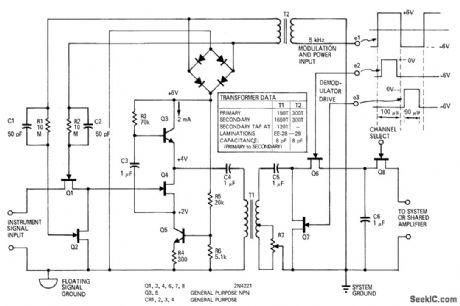
Combination of 5-kHz FET-chopper amplifier Q1-Q2 with transformer isolation of signal and system grounds gives low-cost analog instrumentation amplifier that will process millivolt DC signals while rejecting hundreds of volts of common-mode DC. Signal accuracy is 0.1% for inputs between 50 and 500mV. Input impedance is 4 megohms, drift is only 0.2μV/℃, and DC common-mode rejection rate is better than 120 dB. Low-impedance output of followers Q3-Q4-Q5 is sent through T1 to synchronousFET demodulator Q6-Q7,R7 adjusts system scaling.C.A.Walton,High-CMR,Low-Cost DC Instrumentation Preamp,EDN Magazine,Jan 15,1971,p 47-48. (View)
View full Circuit Diagram | Comments | Reading(779)
PEAK_DETECTOR
Published:2009/7/10 3:28:00 Author:May

A 0-to-5 V input drives the negative input of LM392 comparator if reset (pin 12) if DC4060BE is pulled high then low, all outputs of ICF1 are forced low, forcing + input of comparator to go low. Q1 is cut off and 101's clock oscillator, running at about 775 Hz, starts counting. The Q4 through Q14 outputs con-nect to a ladder. When the counter reaches a count so that the voltage on pin 3 of the LM392 equals the peak input voltage, the counter stops. This voltage is available at the output of the voltage follower LM392 (pin 7). The maximum time to acquire a peak is 22 seconds. This circuit is slow and was originally intended for battery-charging applications. (View)
View full Circuit Diagram | Comments | Reading(0)
HALL_SENSOR_CURRENT_MONITOR
Published:2009/7/10 3:28:00 Author:May


The circuit uses a Hall-effect sensor, which consists of an IC that resides in a small gap in a flux-collector toroid, to measure dc current from 1 to 40 A. Wrap the current-carrying wire through the toroid; the Hall voltage VH is then linearly proportional to the current (I). The current drain from VB is less than 30 mA.
To monitor an automobile alternator's output current, for example, connect the car's battery between the circuit's VB terminal and ground, and wrap one turn of wire through the toroid (or, you could wrap 10 turns-if they'd fit-to measure 1 A full-scale). When I=0V, the current sensor's (CS1's) VH output equals one-half of its 10-V bias voltage, VH and VOUT are zero when I is zero; you can then adjust the output gain and offset to scale VOUT at 1V per 10A (View)
View full Circuit Diagram | Comments | Reading(3286)
ON_OFF_INVERTERS
Published:2009/7/10 3:27:00 Author:May

Each time the switch closes, the voltage on C1 causes inverter A to change state, with positive feedback from inverter B. Resistor R1 delays the charging and discharging of C1, making the circuit virtually immune to contact bounce. The circuit works with either CMOS or TTL gates. The values of R1 and C1 are not critical and can be increased for greater contact bounce protection, if needed.Recommended ranges are 10 K to 1 MΩ for R1, and 0.01 to 1.0 μF for C1. (View)
View full Circuit Diagram | Comments | Reading(735)
WIEN_BRIDGE_OSCILLATOR
Published:2009/7/10 3:26:00 Author:May

The HA2541 is well-suited for use as the heart of an oscillator. In spite of the rudimentary diode limit-ing that is provided by R3 through R7 and Dl and D2, a good-quality sine wave of 40 MHz is readily attain-able with an upper limit of 50 MHz, which exceeds the unity-gain bandwidth of HA-2541.
R1/C1 and R2/C2 provide the required regenerative feedback needed for adequate frequency stability.In theory, the feedback network requires a gain of three to sustain oscillation. However,the practical gain needed is just over three and is provided by R8 and R9. (View)
View full Circuit Diagram | Comments | Reading(0)
ONE_MOSPOWER_FET_ANALOG_SWITCH
Published:2009/7/10 3:26:00 Author:May

Using four diode in an array allows using only one MOSPOWER transistor for analog switching.The current flow is controlled by keeping the source-base connection of the MOSFET towards the load. Be sure to use diodes capable of handling the load current and a transistor whose breakdown voltage specification exceeds the peak analog voltage anticipated. Operationally, by increasing the gate-to-source bias voltage, the MOSFET turns on. For applications other than either full-on or full-off, care must be taken not to exceed the dissipation of the MOSPOWER transistor. A suitable heatsink cannot be overstressed in such applications. (View)
View full Circuit Diagram | Comments | Reading(794)
| Pages:830/2234 At 20821822823824825826827828829830831832833834835836837838839840Under 20 |
Circuit Categories
power supply circuit
Amplifier Circuit
Basic Circuit
LED and Light Circuit
Sensor Circuit
Signal Processing
Electrical Equipment Circuit
Control Circuit
Remote Control Circuit
A/D-D/A Converter Circuit
Audio Circuit
Measuring and Test Circuit
Communication Circuit
Computer-Related Circuit
555 Circuit
Automotive Circuit
Repairing Circuit