
Circuit Diagram
Index 826
CONSTANT_OUTPUT_OSCILLATOR
Published:2009/7/19 21:26:00 Author:Jessie

Used with automatic doppler cycle counter to determine position and velocity of missiles and satellites. Output signal amplitude is maintained constant over wide range of maintained constant over wide range of frequencies. –B. E. Keiser, Digital-Counter Techniques Increase Doppler Uses, Electronics, 32:21, p 46-50. (View)
View full Circuit Diagram | Comments | Reading(655)
MULTI_OUTPUT_BINARY
Published:2009/7/19 21:26:00 Author:Jessie

Basic binary circuit of 256-channel neutron analyzer is controlled by diode gates in coincidence with dock pulses derived from 200-kc crystal oscillator. Used in countdown, address overflow, memory cycle, sync, and gate stages.-E. J. Wade, Digital Instrumentation for Nuclear Research Tests, Electronics, 33:43, p 68-71. (View)
View full Circuit Diagram | Comments | Reading(571)
Precision_voltage_sourced_VFC
Published:2009/7/19 21:25:00 Author:Jessie

Figure 12-3 shows a voltage-sourced VFC that is similar to Fig. 12-2, except that current pulses into the integrator are taken directly from the switched voltage reference. This improves temperature drift at the expense of high-frequency linearity. Raytheon Linear Integrated Circuits, 1989, p 7-8 (View)
View full Circuit Diagram | Comments | Reading(555)
Noninverting_amplifier_using_half_of_an_ECG947_dual_operational_amplifier
Published:2009/7/19 21:25:00 Author:Jessie

Noninverting amplifier using half of an ECG947 dual operational amplifier. The ECG947 is short-circuit protected and requires no external components for frequency compensation (courtesy GTE Sylvania Incorporated). (View)
View full Circuit Diagram | Comments | Reading(531)
0_66V_AT_2A
Published:2009/7/19 21:24:00 Author:Jessie

High-power circuit is suitable for low-voltage logic devices that require high current at supply voltages between 3 and 6V. Maximum output of 2A is obtained with 2N6057 Darlington pair for Q1. Single 2N3766 can be used if load is only 100mA. Q2 provides short-circuit protection for Q1, Since supply does not have to be adjusted down to 0V,negative supply for A2 can go to common negative of circuit. Optional connection to -3 V is used only when voltage range must go down to 0V.-W.G. Jung, IC Op-Amp Cookbook, Howard W. Sams, Indianapolis, IN, 1974, p 157-158. (View)
View full Circuit Diagram | Comments | Reading(721)
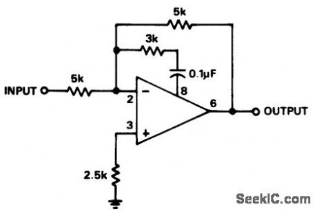
General_purpose_operational_amplifier_with_closed_loop_gain_greater_than_10
Published:2009/7/19 21:24:00 Author:Jessie

General-purpose operational amplifier with closed-loop gain greater than 10. Typical supply voltage is ±15 volts (courtesy Analog Devices, Inc.). (View)
View full Circuit Diagram | Comments | Reading(580)
Precision_current_sourced_VFC
Published:2009/7/19 21:23:00 Author:Jessie

Figure 12-2A shows a current-sourced VFC that is similar to Fig. 12-1, except that the passive RC integrator is replaced by an active op-amp integrator.This increases the dynamic range down to 0 V, improves response time, and eliminates the nonlinearity error that is introduced by the limited compliance of the switched current source output. Figure 12-2B shows the operating range for various component values. Raytheon Linear Integrated Circuits 1989 p 7-7, 7-8. (View)
View full Circuit Diagram | Comments | Reading(567)
10_CPS_PHASE_SHIFT_FET_OSCILLATOR
Published:2009/7/19 21:23:00 Author:Jessie

Uses four-mesh feedback network to provide attenuation of 18:36, without use of lamps. –V. Glover, Using a New Device: Field-Effect Transistor Oscillators, Electronics,35:51, p 44-46. (View)
View full Circuit Diagram | Comments | Reading(606)
NEUTRON_DIFFRACTOMETER
Published:2009/7/19 21:23:00 Author:Jessie

Neutron beam from reactor strikes sample, producing diffraction pattern. Multielement glow tubes control sequence of operation in which length of data accumulation time at each angle of diffraction is determined by counting neutrons in incident beam. This eliminates counting errors due to reactor level fluctuations. Circuit drives key solenoids of electric type-writer to give printout of results.-E. W. Johanson, Glow-Tube Programmer Controls Neutron Spectrometer Experiments, Electronics, 34:19, p 65-67. (View)
View full Circuit Diagram | Comments | Reading(617)
SLAVE_FLASH_TRIGGER
Published:2009/7/10 3:54:00 Author:May

The SCR is wired across the trigger circuit of the flash gun. Normally, the SCR is off, so the flash gun is able to charge to its trigger voltage. Photo transistor Q1 is used to monitor the light level.When a high-intensity flash occurs, Q1 briefly con-ducts and supplies gate current to the SCR. That causes the SCR to turn on, which then triggers the slave flash gun via the hot-shoe adapter terminals.
0nce the flash gun has triggered, the SCR's quickly tums off again. That happens because the current in circuit quickly falls below the SCR's hold-ing current. The resistor at the base of Q1 (R1)determines the sensitivity of the circuit. If you wish, you can reduce the sensitivity, simply by reducing the value of the resistor from that shown.The 1-kΩ resistor between the gate and cathode of the SCR (R3) prevents the SCR from false trigger-ing if high voltages are applied between the anode and the cathode. Q1 can also be a GEL14G2. (View)
View full Circuit Diagram | Comments | Reading(2160)
Instrument_amplifier_using_an_AD521_op_amp
Published:2009/7/19 21:23:00 Author:Jessie
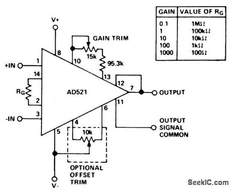
Instrument amplifier using an AD521 op amp. Typical supply is±15 volts (courtesy Analog Devices, Inc.). (View)
View full Circuit Diagram | Comments | Reading(804)
LOW_OHMS_ADAPTER
Published:2009/7/10 3:53:00 Author:May

The circuit consists of a 5-V regulator, constant-current source D1, D2, and Q1, and op amp gam stage U1. Power is provided by a 9-V battery whose output is regulated to + 5 Vdc by the 3-terminal regu-lator. The emitter of Q1 is always 0.6 V below the + 5-V line. Resistor R1 sets the current through both diodes D1 and D2 to 5mA.
The resulting 0.6 Vdc across one of the multiturn trimmer potentiometers (R2 and R3), as selected by switch section S2A, sets the current through Q1 and the resistor-under-test.
When R2 is selected, the test current is 1mA; when R3 is selected, the test current is 10mA. On the lower two ranges, ×1 and ×10, the voltage across resistance-under-test is applied directly to the DMM terminals. On the upper two ranges, op amp gain stage UI is switched into the circuit and the DMM mea-sures the voltage between op amp output pin 6 and the test resistor.
When switch S2 is in position 3 (× 100) the current set by the constant-current source is 1 mA; the multiplying factor is ×100. When S2 is in position 4, ×1 000, the current is 10 mA and the multiplying factor is 100 x 10 = 1 000. Multiturn trimmer-potentiometer R6 adjusts the offset of the op amp so that, with no voltage across the resistor-under-test (i.e. with the measurement terminals short-circuited), the output is zero. (View)
View full Circuit Diagram | Comments | Reading(887)
HIGH_INPUT_IMPEDANCE
Published:2009/7/10 3:50:00 Author:May


Two-opamp conoutput nection shown gives input resistance of 200 megohms and drift time of 90 min for0 to 10 V.-N. G. Boreham, Op-Amp Integrator, Wireless World, March 1977, p 42. (View)
View full Circuit Diagram | Comments | Reading(3126)
Op_amp_with_high_bandwidth_using_an_AD5188_pin_TO99_Bandwidth_is_nearly_25MHz_with_the_feed_forward_technique_shown
Published:2009/7/19 21:22:00 Author:Jessie
Op amp with high bandwidth using an AD5188-pin TO99, Bandwidth is nearly 25MHz with the feed forward technique shown(courtesy Analog Devices, Inc.). (View)
View full Circuit Diagram | Comments | Reading(543)
CODE_PRACTICE_OSCILLATOR
Published:2009/7/19 21:22:00 Author:Jessie

Requires only single flashlight cell and two transistors. - Transistor Manual, Seventh Edition, General Electric Co., 1964, p 378. (View)
View full Circuit Diagram | Comments | Reading(0)
NEGATIVE_SHUNT_REGULATION
Published:2009/7/19 21:22:00 Author:Jessie

Connection shown for LM117 positive series regulator provides spike-suppressing negative shunt regulation of -5V output With capacitor shown, regulator will withstand 75-V spikes on raw DC supply For larger spikes, increase capacitor value.-P Lefferts, Series Regulators Provide Shunt Regulation, EDN Magazine, Sept 5,1978,p158 and 160. (View)
View full Circuit Diagram | Comments | Reading(653)
Instrumentation_amplifier_using_two_AD5108_pin_TO99_op_amps
Published:2009/7/19 21:22:00 Author:Jessie
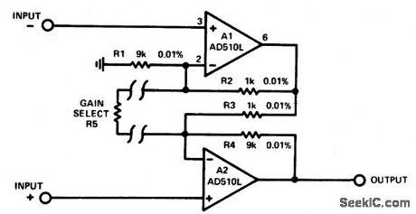
Instrumentation amplifier using two AD5108-pin TO99 op amps.As shown the gain is 10. By adding R5 the gain will increase. For a gain of 10 the frequency response is down 3 dB at 500 kHz. Full output of ±10 volts can be attained up to 1800 hertz(courtesy Analog Devices, Inc.). (View)
View full Circuit Diagram | Comments | Reading(483)
Basic_voltage_to_frequency_converter
Published:2009/7/19 21:22:00 Author:Jessie

Figure 12-1A shows a stand-alone VFC. Figure 12-1B shows the operating range for various component values. This single-supply VFC is recommended for uses, where the dynamic range of the input is limited, and the input does not reach 0 V. Raytheon Linear Integrated Circuits, 1989 p 7-6 7-7 (View)
View full Circuit Diagram | Comments | Reading(620)
30_MC_2N2188
Published:2009/7/19 21:21:00 Author:Jessie

Delivers 23 mw over temperature range of -40 to +60℃. Typical collector efficiency is 30%.-Texas Instruments Inc., Transistor Circuit Design, McGrctw-Hill, N.Y., 1963, p 319. (View)
View full Circuit Diagram | Comments | Reading(611)
5V_AT_5A_FOR_TTL
Published:2009/7/19 21:21:00 Author:Jessie

Typical load regulation is 1.8% from no load to full load, Q1 and Q2 serve in place of single higher-cost power PNP boost transistor. Dotted lines show how to add overload indicator using National NSL5027 LED and R2 as overload sensor. When load current exceeds 5A, Q3 turns on and D3 lights. Circuit includes thermal shutdown and short-circuit protection.- Linear Applications, Vol. 2, National Semiconductor, Santa Clara, CA, 1976, AN-103, p 5. (View)
View full Circuit Diagram | Comments | Reading(801)
| Pages:826/2234 At 20821822823824825826827828829830831832833834835836837838839840Under 20 |
Circuit Categories
power supply circuit
Amplifier Circuit
Basic Circuit
LED and Light Circuit
Sensor Circuit
Signal Processing
Electrical Equipment Circuit
Control Circuit
Remote Control Circuit
A/D-D/A Converter Circuit
Audio Circuit
Measuring and Test Circuit
Communication Circuit
Computer-Related Circuit
555 Circuit
Automotive Circuit
Repairing Circuit