
Circuit Diagram
Index 824
SCR_POWER_MONITOR
Published:2009/7/10 4:10:00 Author:May

Pressing R1 lights I1, which will extinguish if there has been a power failure. (View)
View full Circuit Diagram | Comments | Reading(700)
_10V_AT_2A
Published:2009/7/19 21:35:00 Author:Jessie

Negative-voltage regulator using SN52104 or SN72304 accepts input voltage of -12V to -40V and uses only single external resistor to provide regulated output of -10 V with typical load regulation of 1mV and input regulation of 0.06%. ICs are interchange-able with LM104 and LM304 respectively.- The Linear and Interface Circuits Data Book for Design Engineers, Texas Instruments, Dallas, TX, 1973, p 5-5. (View)
View full Circuit Diagram | Comments | Reading(1747)
Single_pole_frequency_compensation_circuit_using_an_AD101A_201A_301A_op_amp
Published:2009/7/19 21:34:00 Author:Jessie
Single pole frequency compensation circuit using an AD101A/201A/301A op amp. Typical supply voltage is ±15volts. Voltage gain is 88 dB (courtesy Analog Devices, Inc.). (View)
View full Circuit Diagram | Comments | Reading(467)
HIGH_RESISTANCE_MEASURING_DMM
Published:2009/7/10 4:09:00 Author:May


Using a simple technique, you can extend the resistance-measurement range of your 31/2-digit DMM from the usual 19.99 MΩ to 40 GΩ. You could measure, for example, the leakage resis-tances of transformers, motor windings, and capacitors.
For a 19.99-MΩ DMM range, select a stable 20-MΩ resistor whose value is slightly below nomi-nal, 19.99 MΩ for example. An unknown high resistance, RX,is:
where Rp is the high-value parallel resistor and RpX is the measured value of Rp in parallel with RX. An even easier way to determine the value of Rx is to use the graph. (View)
View full Circuit Diagram | Comments | Reading(791)
STORING_INTEGATOR_OUTPUT
Published:2009/7/10 4:07:00 Author:May

Modifiedsample-and-hold circuit with capacitive feed-back combines integrate,sample,and holdfunctions,fotuse In temporarily storing output of integrator Integrating amplifieris 741 opamp; for critical applications,FET opamp is preferable.-E. crovella, Circuit Combines Integrate,Sample and Hold Functions,EDN Magazine,Oct,20,1974, p 90. (View)
View full Circuit Diagram | Comments | Reading(609)
5_VSUPPLY_HIGH_SIDE_SWITCHER
Published:2009/7/10 4:07:00 Author:May


Requiring only 10 uA of quiescent current, the circuit of (Fig. 62-1(a)) produces only 0.1-Ω ON-resis-tance. IC1 is a charge pump voltage converter to produce a -5-V level, so analog switch IC2 can provide a 10-V swing to MOSFET Q1.
This circuit uses a voltage converter to enable the analog switch to apply a 4.3-V swing to logic level NMOS power transistor Q1. ON resistance is 0.03 Ω typical.
This circuit uses additional stages in the voltage-multiplying circuit to provide a higher gate voltage swing. This would enable the use of a convener for an NMOS switching transistor. (View)
View full Circuit Diagram | Comments | Reading(656)
SCS_RLC_OSCILLATOR
Published:2009/7/19 21:34:00 Author:Jessie

Positive transient, such as closing of switch, charges C through L. When current reverses, diode blocks and triggers scs. When capacitor discharges, scs turns off and C charges to repeat cycle.- Transistor Manual, Seventh Edition, General Electric Co., 1964, p 434. (View)
View full Circuit Diagram | Comments | Reading(699)
Voltage_to_frequency_converter_with_zero_and_full_scale_adjust
Published:2009/7/19 21:34:00 Author:Jessie

This circuit shows a VFC with both zero and full-scale adjustments.Raytheon Linear Integrated Circuits, 1989 p 7-20 (View)
View full Circuit Diagram | Comments | Reading(622)
Unity_gain_feed_toward_amplifier_using_an_MC1539_op_amp
Published:2009/7/19 21:33:00 Author:Jessie
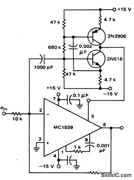
Unity-gain feed toward amplifier using an MC1539 op amp (courtesy Motorola Semiconductor Products Inc.). (View)
View full Circuit Diagram | Comments | Reading(554)
IC_PRODUCT_DETECTORS
Published:2009/7/10 4:06:00 Author:May

These product detectors use IC devices. SSB and CW signals can be detected with them. The circuits should be useful up to 20 or 30 MHz. T3 in (c) is a 1:1:1 toroidal type, depending on the BF0 frequency. (View)
View full Circuit Diagram | Comments | Reading(1387)
RING_OF_FIVE_NEON_OSCILLATOR
Published:2009/7/19 21:33:00 Author:Jessie

Can be used for sequential switching, with operating cycles of various lengths at audio and subaudio frequencies. When first turned on, one of lamps fires because of inequalities in lamp properties, and others then fire in sequence. Values of R and C determine cycle duration, according to formula given in article. Time is 1 sec for C=0.5 mfd and R=10 meg.-R. L. lves, Neon Oscillator Rings, Electronics, 31:41, p 108-115. (View)
View full Circuit Diagram | Comments | Reading(774)
VARIABLE_DUTY_CYCLE_SQUARE-WAVE_GENERATOR
Published:2009/7/10 4:06:00 Author:May
C1 alternately charges via R1/D1 and the upper half of R5, and discharges via R1/D2 and the lower half of R5. The duty cycle can be varied over the range from 1:10 to 10:1 via R5. (View)
View full Circuit Diagram | Comments | Reading(928)
Summing_amplifier_using_an_MC1539_op_amp
Published:2009/7/19 21:33:00 Author:Jessie
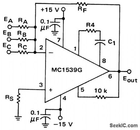
Summing amplifier using an MC1539 op amp (courtesy Motorola Semiconductor Products Inc.). (View)
View full Circuit Diagram | Comments | Reading(641)
Unity_gain_operational_amplifier
Published:2009/7/19 21:32:00 Author:Jessie

Unity-gain operational amplifier. With the compensation shown a unity-gain frequency of approximately 10 MHz to 12 MHz results (courtesy Analog Devices, Inc.). (View)
View full Circuit Diagram | Comments | Reading(571)
Frequency_to_voltage_converter_with_zero_and_full_scale_adjust
Published:2009/7/19 21:32:00 Author:Jessie

This circuit shows an FVC with both zero and full-scale adjustments.Raytheon Linear integrated Circuits 1989 p 7 19 (View)
View full Circuit Diagram | Comments | Reading(625)
STABLE_3_MC_CRYSTAL_COLPITTS
Published:2009/7/19 21:32:00 Author:Jessie

Crystal operates at series resonance in feedback path between emitter of Q2 and tank tap. Q1 is shunt voltage regulator providing power-supply isolation. Two-stage feedback amplifier Q3-Q4 provides output impedance of about 150 ohms when R1 is adjusted for 0.5-V peak-to-peak output swing.-J. W. Hamblen and J. B. Oakes, Instrumentation and Telemetry of Transit Navigational Satellites, Electronics, 34:32, p 148-153. (View)
View full Circuit Diagram | Comments | Reading(609)
1_99900_μF
Published:2009/7/10 4:05:00 Author:May

Circuit converts charging time of unknown capacitor to capacitance value shown on 3-digit display. S-1 is shown in OFF position, with unknown capacitor shorted. When S-1 is changed to other position for start of test, Cx is connected to measuring circuit through range switch S-2 and 741 opamp used as comparator. 60-Hz timing waveform is now applied to sinewave squaring circuit using two sections of 7408 AND gate. This starts 7490 counters. Zener-regulated +9 V is applied to Cx through selected range resistor .When charging voltage of capacitor exceeds reference voltage on inverting input, 741 output goes positive andstops counter, Article describes circuit operation in detail. Range switch glves scaling factors of 1,10,100,and 1000.-A,s Joffe,Now-aDigital Capacity Meter!, 73 Magazine, May1978,p 58-60. (View)
View full Circuit Diagram | Comments | Reading(1586)
Inverting_only_composite_op_amp
Published:2009/7/19 21:31:00 Author:Jessie
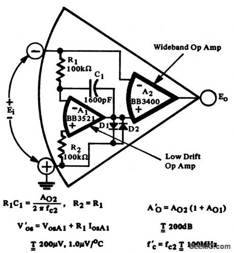
Inverting-only composite op amp (courtesy Burr-Brown Research Corporation). (View)
View full Circuit Diagram | Comments | Reading(722)
0_25V_AT_0_10A
Published:2009/7/19 21:30:00 Author:Jessie

Lab-type constant-voltage/constant-current power supply using standard ICs achieves high current output by paralleling of seven LM395 power transistors serving as pass element. Current limiting is provided on LM395 chip for complete overload protection.- Linear Applications, Vol. 2, National Semiconductor, Santa Clara, CA, 1976, LB-28. (View)
View full Circuit Diagram | Comments | Reading(2983)
SQUARE_WAVE_OSCILLATOR
Published:2009/7/10 4:02:00 Author:May


The NE555 is connected in the astable mode and uses only three timing components (RA, RB, and Ct. A 0.01-μF bypass capacitor is used on pin 5 for noise immunity. The operating restrictions of the astable mode are few. The upper frequency limit is about 100 kHz for reliable operation, as a result of internal storage times. Theoretically, it has no lower frequency limit, only that which is imposed by Rt and Ct limitations. The frequency for the circuit can be calculated as: (View)
View full Circuit Diagram | Comments | Reading(0)
| Pages:824/2234 At 20821822823824825826827828829830831832833834835836837838839840Under 20 |
Circuit Categories
power supply circuit
Amplifier Circuit
Basic Circuit
LED and Light Circuit
Sensor Circuit
Signal Processing
Electrical Equipment Circuit
Control Circuit
Remote Control Circuit
A/D-D/A Converter Circuit
Audio Circuit
Measuring and Test Circuit
Communication Circuit
Computer-Related Circuit
555 Circuit
Automotive Circuit
Repairing Circuit