
Circuit Diagram
Index 829
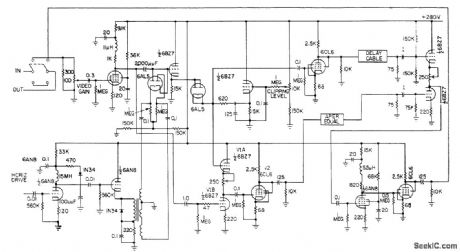
RADIOLOGICAL_VACUUM_GAGE
Published:2009/7/19 21:52:00 Author:Jessie

Permils measuring extremely low pressures in laboratory equipment and in high-althude research. Provides digital output that can be used for storage for telemetry. Transformer is audio type with Iarge step-up ratio. Polarizing voltage supplies less than 1 microamp. Transducer is small cylindrical tube lined with radioactive foil.-G. F. Vanderschmidt, Using lsotopes to Measure tow Pressures, Electron-ics, 32:25, p 60-61. (View)
View full Circuit Diagram | Comments | Reading(718)
_15_5AND__15V
Published:2009/7/19 21:52:00 Author:Jessie


Single potentiometer R5 serves for adjusting all three regulated output voltages simultaneously Accuracy of adjustment is within 2%.-R.C Dobkin. One Adjustment Controls Many Regulators .EDN Magazine,Nov,1,1970,p33-35 (View)
View full Circuit Diagram | Comments | Reading(626)
Tachometer_with_set_point
Published:2009/7/19 21:51:00 Author:Jessie

This circuit shows an ICLT182 bargraph converter that is connected to form a tachometer with set point. The connections between the ICL7182 and bargraph are shown in Fig. 12-14. Harris Semiconductor$ Data Acquisition 1991 p 2 144 (View)
View full Circuit Diagram | Comments | Reading(0)
SURVEY_METER_HAS_PULSED_AND_CURRENT_MODES
Published:2009/7/19 21:51:00 Author:Jessie

High-voltage source for G-M counter uses 10-kc blocking oscillator and Cockcroft-Walton multiplier, to give 550 v stabilized by zener region of D1. Range for pulsed operation is 0.5 to 50 milliroentgen per hour. For current mode, same 18503 G-M tube is used, and current in range of 50 milliroentgen to 5 roentgen per hour is logarithmic function of radiation intensity.-R. W. Lehnert and J. M. McKenzie, Radiation Survey Meter, Electronics, 35:8, p 50. (View)
View full Circuit Diagram | Comments | Reading(869)
PERFERRED_PULSE_FREQUENCY_DIVIDER_
Published:2009/7/19 21:50:00 Author:Jessie

Blocking oscillator design produces equally spaced pulses at submultiple of 2 to 5 of trigger frequency. Maximum prf is 2,000 pps. Input und output are both positive. Plate voltage is 300 V with 5814A tube and 150 V with 6111. R6 is 100 or 150 ohms depemding on tube. R7 should be maximum that will just suppress ringing,-NBS, Handbook Preferred Circuits Navy Aeronautical Electronic Equipment, Vol. I, Electron Tube Circuits, 1963, PC 50, p 50-2. (View)
View full Circuit Diagram | Comments | Reading(648)
Bargraph_display_of_quad_load_cell_values
Published:2009/7/19 21:50:00 Author:Jessie

This shows an ICL7182 bargraph converter connected to measure ratiometric values of quad load cells, and to display the results on a bargraph. The resistor values within the load-cell bridge are determined by the desired sensitivity.Harris Semiconductors, Data Acquisition 1991 p. 2-143 (View)
View full Circuit Diagram | Comments | Reading(3234)
10_bit_multiplying_D_A_convener_in_bipolar_operation
Published:2009/7/20 4:26:00 Author:Jessie

10-bit multiplying D/A convener in bipolar operation. In this configuration the D/A converter is set up for four-quadrant multiplication (courtesy Analog Devices, Inc.). (View)
View full Circuit Diagram | Comments | Reading(894)
CAMERA_HIGHLIGHT_EQUALIZER
Published:2009/7/20 1:28:00 Author:Jessie
Provides better signal-to-signal noise ratio and improved definition over conventional aperture equalizers covering full brightness range. Since most image orthicon noise is in low light region, improvement is achieved by dividing signal into two parts and equalizing only relatively quiet highlight portion. Complete video signal is amplified and applied to white clipper and to difference amplifier V1-V2. Horizontal drive is also applied to clamp portion of circuit. Video signal is clamped at white clipper, where high-lights are clipped from signal-M. V. Sullivan, Highlight Equalizer Sharpens Tv Pictures, Electronics, 31:3, p 72-74. (View)
View full Circuit Diagram | Comments | Reading(735)
AM_ENVELOPE_DETECTOR
Published:2009/7/10 3:47:00 Author:May


This general-purpose detector for AM enve-lope detection can be used in many receiver appli-cations. T1 matches the IF amplifier impedance (typically 1 to10 kΩ) to the 1 kΩ (approximately) detector impedance. Dl can be an IN60, IN82AG, IN270, or a similar type. (View)
View full Circuit Diagram | Comments | Reading(1188)
FAST_DUMP_SWITCH_
Published:2009/7/10 3:46:00 Author:May


Requires only 350 ns to dump 6-V output to level of 3 mV. Transistors are connected so one of them is biased in forward mode independently of output polarity. Both transistors tum on during dump interval.Transistor operating in forward mode determines initial discharge rate until it saturates, after which inverted-mode transistorcontinuesto discharge capacitor. Offset voltage error is only -25 μV. Opamp is Analog Devices 120 or equivalent having unityqain bandwidth above 100 MHz and slew rate above 200 V/us.-F. Tarico, Fast Bipolar Dump Switch Has Low Offset, EDN Magazine,Nov5,1974.p 66. (View)
View full Circuit Diagram | Comments | Reading(651)
DETECTOR_AND_CONTROLLER
Published:2009/7/10 3:46:00 Author:May
Many applications require analog signals to be sensed and digital signals to be controlled. A way to detect these points is by using a 555 timer in an unconventional configuration. This method will also add hysteresis to the circuit and guard against oscillation. The 555 supplies two comparators and a flip-flop eliminates the oscillation. Using this classic timer in the new configuration also reduces the component count.
The circuit shows the 555's trigger and threshold pins tied together. This enables the comparators to set and reset the flip-flop. Op amp U2 supplies both the trip-point setting and a way to adjust the hysteresis for ON and OFF points. One application where this circuit would be useful is in a Nicad battery-charge controller. (View)
View full Circuit Diagram | Comments | Reading(548)
QUICK_MULTICONDUCTOR_CABLE_TESTER
Published:2009/7/10 3:45:00 Author:May

This circuit can be used to check up to an eight-conductor cable. IC1, a 555 timer, drives decade counter 1C2, a 4017. Each LED should light in sequence. The cable to be tested is connected between PL1 and PL2. If the cable is miswired, the LEDs will light out of sequence. If it is shorted or open, some LEDs will not light. (View)
View full Circuit Diagram | Comments | Reading(1840)
CAMERA_TRIP_CIRCUIT
Published:2009/7/10 3:44:00 Author:May

This circuit was used to trip a camera shutter. Grounding pin 2 of U1 makes pin 4 of U1 go high. This triggers both timers of dual timer U1. One output holds reset (pin 4) of U1 low to keep U1 from accepting another trigger, depending on the time constant of R7 and C3. This prevents camera film waste. The other timer is used to generate a 1/2-second pulse to drive U4 and Q1, the relay driver. K1 triggers the camera. (View)
View full Circuit Diagram | Comments | Reading(534)
SIMPLE_TTL_LSTTL_CMOS_SQUARE_WAVE_GENERATORS
Published:2009/7/10 3:43:00 Author:May


These three circuits for TTL. LSTTL. and CMOS logic use three gates each, and one or two resistors and capacitor as a square-wave oscillator. The circuits are useful for clock oscillators, etc. R and C are determined from the nomographs (View)
View full Circuit Diagram | Comments | Reading(1489)
CONTINUITY_TESTER
Published:2009/7/10 3:42:00 Author:May

Using an LED and an audible indicator, relay K1 actuates buzzer BZ1. S2 is a buzzer/battery test switch for testing the battery in both NO and NC mode. (View)
View full Circuit Diagram | Comments | Reading(0)
LOW_LEVEL_DIODE_ENVELOPE_DETECTOR
Published:2009/7/10 3:41:00 Author:May

An approach to low-level RF detection and performance curves is shown here. This design is for 10 MHz, but values can be scaled to other frequencies, if needed. (View)
View full Circuit Diagram | Comments | Reading(739)
INTEGATE_AND_DUMP
Published:2009/7/10 3:41:00 Author:May

Transistor is used as switch, without power supply. Simple RC integrator will dump (discharge C) completely in about 1 μs when dump input is logic 1 (+5 V).Values of R and C determine time constant of integrator. Without power supply, circuh can only drive high-impedance load; for low-impedance load, add FET-input opamp such as Analog Devices 40J as buffer.-R. Riordan, Integrate and Dump Circuit Uses No Power Supply, EDN Magazine, Feb. 20, 1973, p 93. (View)
View full Circuit Diagram | Comments | Reading(2683)
CONTINUITY_CHECKER
Published:2009/7/10 3:41:00 Author:May

U1 is an op amp used as a comparator. When the test probes are shorted together, resistors R1 and R2 bias the noninverting input to half the supply voltage. The inverting input is biased by a voltage divider that consists of R3, R7, and R4. Resistor R7 is adjusted so that the voltage to the inverting input is lower than that to the noninverting input when the probes are shorted together. With continuity across the probes, U1's output goes high and supplies power to Q1, which is configured as arelaxation oscillator. The output of Q1 is fed to a high-impedance loudspeaker for an audio tone. When the probe is open, the nonin-verting input goes to the negative supply rail via R2. This action forces U1 is output low, which results in no output from the oscillator. (View)
View full Circuit Diagram | Comments | Reading(2085)
NOAA_WEATHER_ALERT_DECODER
Published:2009/7/10 3:39:00 Author:May

This circuit detects the 1050-Hz tone sent by the NOAA (National Oceanic and Atmospheric Adminis-tration) Weather radio stations that operate from 162.40 to 162.55 MHz. This tone lasts for several sec-onds. Q1 is an amplifter that feeds tone detector U1, an NE567 detects this tone and produces a low on pin 8. This is coupled to a 555 timer (U3), which produces a high on its pin 3, sounds BZ1, triggers SCR1, and lights the LED. S2 is used to rest the circuit.
Audio is taken from the receiver that is used with the device. S1 is used to test the device and it will sound the alarm in two seconds if all is OK., (View)
View full Circuit Diagram | Comments | Reading(1301)
TIME_DELAY_PHOTO_FLASH_TRIGGER
Published:2009/7/10 3:39:00 Author:May

Q1 is a phototransistor that is normally illuminated by a beam of light. When the beam is intercoupled, pin 1 of U1A goes high, and forces pin4 U2B low. Then, C2 discharges through R2 and R3. After a certain time delay, pin 10 U1C goes high, triggers SCR1, and sets off the flash. R4/C1 charges, causes U1D out-put to go low after about 1/2 second, and resets U1A and U1B to the initial state. This delay prevents accidental double flash exposure. (View)
View full Circuit Diagram | Comments | Reading(807)
| Pages:829/2234 At 20821822823824825826827828829830831832833834835836837838839840Under 20 |
Circuit Categories
power supply circuit
Amplifier Circuit
Basic Circuit
LED and Light Circuit
Sensor Circuit
Signal Processing
Electrical Equipment Circuit
Control Circuit
Remote Control Circuit
A/D-D/A Converter Circuit
Audio Circuit
Measuring and Test Circuit
Communication Circuit
Computer-Related Circuit
555 Circuit
Automotive Circuit
Repairing Circuit