
Circuit Diagram
Index 825
Precision_frequency_to_voltage_converter
Published:2009/7/19 21:30:00 Author:Jessie

Figure 12-5 shows an FVC that is similar to Fig. 12-4, except that linearity, offset, and response time is improved by adding an op amp to form an active low-pass filter at the output. Raytheon Linear Integrated Circuits 1989 p 7-10. (View)
View full Circuit Diagram | Comments | Reading(1133)
5_RANGE_LINEAR_SCALE_OHMMETER
Published:2009/7/10 4:02:00 Author:May


Rx is inserted h the feedback path of IC1.A known reference current is selected from reference voltage generator Q1,D1,and R5 through R9.A meter reading will be produced:
where R5=R5 through R9,as selected.This corresponds linearly to the value of Rx. (View)
View full Circuit Diagram | Comments | Reading(820)
ELIMINATING_RINGING
Published:2009/7/10 4:01:00 Author:May

High-Q bandpass integrator reduces ringing significantly by amplifying AC input signal in two broadband differential amplifier stages, A1 and A2 before differentiation and selection by D1 and D2. Input gate pulse P1 and differentiated pulses drive AND logic that generates output pulse Ps coincident with zero crgssings of AC input. Leading edge of Ps will always occur at first zero crossing after P1 initiates gating action. If output drives balanced diode bridge, gating pedestal and AC signal transient are eliminated; high-Q bandpass integrator then has fast settling time, permitting faster repetition rates.-R. J. Tumer, Reduce Integrator Transients with Synchronized Gate Signals, EDN/EEE Magazine, Jan. 15, 1972, p 46-47. (View)
View full Circuit Diagram | Comments | Reading(958)
DIRECT_READING_FIVE_RANGE
Published:2009/7/10 3:58:00 Author:May

Covers 1 pF to 1μF in five ranges, using easily available com ponents. Trigger source is free-running pulse generator using programmable UJT al and inverter-amplifier Q2 to produce narrow -12 V output pulse at constant frequency of about 500 Hz. For trigger pulse, NE555V timer connected as mono MVBR initiates output pulse whose width increases with value of capacitor under test. Meter reads average value of pulse wave form and may be calibrated directly to read capacitance. Range resistors should be 5% or better. 10K trimpot in series with meter serves for initial calibration. Zero-adjustment pot is needed only for lower ranges. Use zener-regu-Iated supply to provide 12 V at up to 50 mA. Full type number of al is A7T6028; 2N6027, 2N6028 2N6118, and HEP S9001 are similar. Single 0.0025-μF capacitor can be substituted for two 0.005-μF units in series.-C. Hall, Direct-Reading Capacitance Meter, Ham Radio, April 1975, p32-35. (View)
View full Circuit Diagram | Comments | Reading(617)
as_CURRENT_INDICATOR
Published:2009/7/10 3:58:00 Author:May

Using a dual op amp driving a rectifier and emitter-follower, this circuit indicates ac current on an LED. L1 is an audio transformer winding using a pick-up coil, or 100 to 200 turns of #28 gauge wire 2 in diameter, etc. The circuit can trace ac lines behind walls, etc. or detect ac current flow. (View)
View full Circuit Diagram | Comments | Reading(4378)
PREFERRED_08_20_MC_ELECTRON_COUPLED_COLPITTS_CRYSTAL
Published:2009/7/19 21:30:00 Author:Jessie

Provides higher output, greater harmonic content, better frequency correlation, and more immunity from effects of load changes than simpler Colpitts version. –NBS, Handbook Preferred Circuits Navy Aeronautical Electronic Equipment, Vol. 1. Electron Tube Circuits, 1963, PC 102, p 102-2. (View)
View full Circuit Diagram | Comments | Reading(760)
Two_pole_frequency_compensation_circuit_using_an_AD101A_201A_301A_op_amp
Published:2009/7/19 21:30:00 Author:Jessie
Two pole frequency compensation circuit using an AD101A/201A/301A op amp.Typical supply voltage is ±15 volts (courtesy Analog Devices, Inc.). (View)
View full Circuit Diagram | Comments | Reading(672)
FALLOUT_TIME_OF_ARRIVAL_INDICATOR
Published:2009/7/19 21:29:00 Author:Jessie

Auto dock operates until fallout at level above 2 milliroentgens per hour arrives. Geiger-counter detection circuit then blows power-supply fuse, stopping clock with hands pointing to time of arrival.-R. W. Farmer and O. Reiner, Jr., Determining Arrival Time of Radioactive Fallout, Electronics, 31:31, p 69-71. (View)
View full Circuit Diagram | Comments | Reading(571)
±15V_AT_7A
Published:2009/7/19 21:29:00 Author:Jessie

External Darlington stages boost output currents of LM125 dual tracking regulator and increase minimum input/output voltage differential to 4.5 V. Maximum output current is limited by power dissipation of 2N3772. Typical load regulation is 40 mV from no load to full load.-T. Smathers and N Sevastopoulos, LM125/LM126/LM127 Precision Dual Tracking Regulators, National Semiconductor, Santa Clara, CA, 1974, AN-82, p 6. (View)
View full Circuit Diagram | Comments | Reading(835)
CODE_PRACTICE_OSCILLATOR_1
Published:2009/7/19 21:28:00 Author:Jessie

Basic tunnel-diode oscillator with single-transistor amplifier stage can be used as code practice oscillator, sensitive broadband c-w keying monitor, sensitive aural-visual parasitic detector, or as wavemeter. - Transisyor Manual, Seventh Edition, General Electric Co., 1964, p 362. (View)
View full Circuit Diagram | Comments | Reading(0)
Clipping_amplifier_using_an_ECG941_941D_941M_operational_amplifier
Published:2009/7/19 21:28:00 Author:Jessie
Clipping amplifier using an ECG941/941D/941M operational amplifier. Typical supply voltage is±15 volts (courtesy GTE Sylvania Incorporated). (View)
View full Circuit Diagram | Comments | Reading(626)
Differential_input_composite_op_amp_
Published:2009/7/19 21:28:00 Author:Jessie
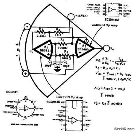
Differential-input composite op amp (courtesy Burr-Brown Research Corporation). (View)
View full Circuit Diagram | Comments | Reading(653)
DIGITAL_WITH_100_1_RANGE
Published:2009/7/10 3:56:00 Author:May

Frequency counter operated in period mode serves as readout for Optical Electronics 3329 voltage-to-frequency converter. Unknown capacitance is connected as external timing capacitance for IC, so output period of IC is directly proportional to unknown capacitance. To calibrate, conned known C and adjust R1 for correct reading on digital frequency counter. With values shown, 1 nF gives period of 1 ms.- Low Cost Capacitance Measurement, Optical Electronics, Tucson, AZ, Application Tip 10262. (View)
View full Circuit Diagram | Comments | Reading(620)
PREFERRED_08_20_MC_COLPITTS_CRYSTAL
Published:2009/7/19 21:27:00 Author:Jessie

Frequency is changed by substituting plug in crystals. Component values depend on frequency range. Serves as simple and stable frequency source.-NBS, Handbook Preferred Circuits Navy Aeronautical Electronic Equipment, Vol. I, Electron Tube Circuits, 1963, PC 101, p 101-2. (View)
View full Circuit Diagram | Comments | Reading(618)
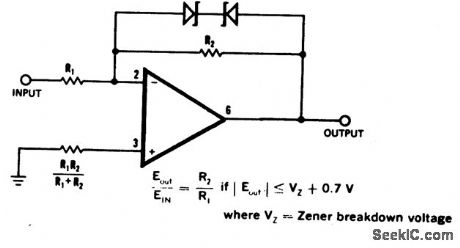
FAST_RECOVERY_
Published:2009/7/10 3:55:00 Author:May

Two diodes and two zeners clamp output of integrator below saturation level of opamp, making recovery time approximately equal to slew rate. With values shown, integration time constant R3 C1 is 35.6 ms and output is clamped at +23 V. Output linearity is ±1%, and threshold range of circuit is -3 V to -10 V.-K. S. Wong, Fast-Recovery Integrator with Adjustable Threshold,EEE Magazine, Aug, 1970, p77. (View)
View full Circuit Diagram | Comments | Reading(608)
PHOTO_RELAY_USES_SR_90_SOURCE
Published:2009/7/19 21:27:00 Author:Jessie

Interruption of high-energy beam from strontium-90 radioactive source changes resistance of cadmium sulphide photocell. Transistor amplifier converts variation into signal that actuates relay or other control element Source-detector separation must be less than 4 inches. Maximum counting rate is five pieces per second.-P. Weisman and S, L. Ruby, Solid-State Photocell Sees Through Haze, Electronics, 31:25, p 62-63. (View)
View full Circuit Diagram | Comments | Reading(586)
SIMPLE_SQUARE_WAVE_OSCILLATOR
Published:2009/7/10 3:55:00 Author:May

Using only four components, this circuit generates a square wave. Oscillation frequency is ≈ 1/ RCx Hz, R=MΩ, Cx-μF (in this case, R=10 kΩ). (View)
View full Circuit Diagram | Comments | Reading(608)
5V_AT_20_A_AND_0_25V_AT_0_24_A
Published:2009/7/19 21:27:00 Author:Jessie

Developed as lab supply for experimenting with high-current TTL circuits. Motorola MC1466 monitors voltage and current requirements monitors voltage and current requirement continuously, providing output proportional to paramenters called for by front-panel controls of supply. D2 and D8 are 50-PIV 20-A diodes, and all other diodes except D3 are 1N4002 or are equivalent. Article give construction detail.- J. W. Crawford, The Smart Power Supply, 73 Magazine, March 1976, p 96-98 and 100-101. (View)
View full Circuit Diagram | Comments | Reading(2880)
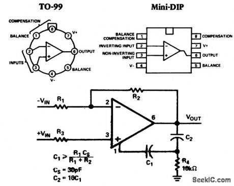
Basic_frequency_to_voltage_converter
Published:2009/7/19 21:27:00 Author:Jessie

Figure 12-4A shows a stand-alone FVC. Figure 12-4B shows the operating range for various component values. This circuit performs the opposite of a VFC (the FVC converts an input pulse train into an average output voltage). Raytheon Linear Integrated Circuits 1989 p. 7-9. (View)
View full Circuit Diagram | Comments | Reading(1293)
Voltage_follower_using_an_MC1556_op_amp
Published:2009/7/19 21:26:00 Author:Jessie
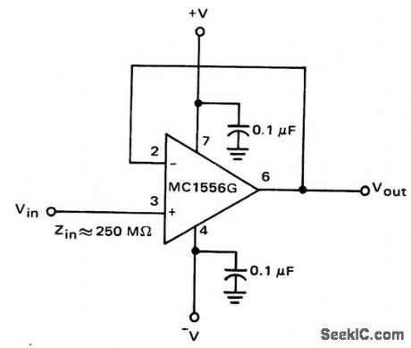
Voltage follower using an MC1556 op amp (courtesy Motorola Semiconductor Products Inc.). (View)
View full Circuit Diagram | Comments | Reading(802)
| Pages:825/2234 At 20821822823824825826827828829830831832833834835836837838839840Under 20 |
Circuit Categories
power supply circuit
Amplifier Circuit
Basic Circuit
LED and Light Circuit
Sensor Circuit
Signal Processing
Electrical Equipment Circuit
Control Circuit
Remote Control Circuit
A/D-D/A Converter Circuit
Audio Circuit
Measuring and Test Circuit
Communication Circuit
Computer-Related Circuit
555 Circuit
Automotive Circuit
Repairing Circuit