Circuit Diagram
Index 820
AUDIO_INDUCTION_RECEIVE
Published:2009/7/10 4:43:00 Author:May

Used to pick up audio signal being fed to low-impedance single-wire loop encircling room or other area to be covered. Pickup loop L1 is 100-500 turns wound around plastic case of receiver. Opamp sections are from Motorola MC3401P or National LM3900 quad opamp. Supply can be 9-15 V. Requires no FCC license. Can be used as private paging system if audio amplifier of transmitter has microphone input.-C. D. Rakes, Integrated Circuit Projects, Howard W. Sams, Indianapolis, IN, 1975, p 23-25. (View)
View full Circuit Diagram | Comments | Reading(1410)
ELECTRONIC_SHUTDOWN
Published:2009/7/19 20:19:00 Author:Jessie

Both sections of National LM125 dual tracking regulatorare shut down by TEL-compatible control signal VT which shorts internal reference voltage of reg-ulatorto ground. Q3 acts only as current sink.-T. Smathers and N. Sevastopoulos, LM125/ LM126/LM127 Precision Dual Tracking Regula-tors, National Semiconductor, Santa Clara, CA, 1974, AN-82, p 15. (View)
View full Circuit Diagram | Comments | Reading(650)
Noninverting_sample_and_hold_circuit_with_gain_equal_to_1__R2_R1
Published:2009/7/19 20:18:00 Author:Jessie

Noninverting sample-and-hold circuit with gain equal to 1 +(R2/R1). The chip is a Datel SHM-IC-1 14-pin DIP. Bandwidth decreases proportionally with gain. R3 is equal to the parallel combination of R1 and R2, and is used to compensate for voltage offset caused by input bias current. R1 and R2 should be 100 PPM/℃ metal film resistors (courtesy Datel Systems, Inc.). (View)
View full Circuit Diagram | Comments | Reading(799)
1_kHz_SQUARE_WAVE_GENERATOR
Published:2009/7/10 4:39:00 Author:May
When the output is high, R3 and R4 are in parallel, and C1 charges via R1 until the current in R2 equals that at the noninverting terminal. This action occurs when C1's voltage rises to 2/3 of the supply voltage. At that point, the circuit switches regeneratively. The output switches low and C1 starts to discharge via R1.Now, R4 is effectively disabled and the current to the noninverting terminal is determined solely by R3, so C1 discharges until the current through R2 falls slightly below that of R3.This happens when the voltage across C1 falls to about 1/3 of the supply voltage. At that point, the circuit again switches regeneratively, and the output again goes high.This circuit is useful for generating symmetrical square waves with maximum frequencies of only a few kHz. Because of the poor slew-rate characteristics of the LM3900 (0.5 V/μs), the output waveforms have rather slow rise and fall times. (View)
View full Circuit Diagram | Comments | Reading(675)
0_TO_166_V_TRACKING_AT_5_mA
Published:2009/7/19 20:17:00 Author:Jessie

Master-slave regulator combination is used to make second regulator provide mirror image of first wllile output of first is varied over full range from 0 to zener limit with R4. Accuracy of tracking de-pends on match between R5 and R6, which should be1 % film or wirewound.-W. G. Jung, IC Op-Amp Cookbook, Howard W. Sams, Indianapolis, IN, 1974, p 160-162. (View)
View full Circuit Diagram | Comments | Reading(624)
BIPOLAR_INPUT_FOR_V_F_CONVERTER
Published:2009/7/10 4:35:00 Author:May

Absolute-value integrator circuit gives effect of generating negative frequencies when input signal is negative by making counter count up for positive voltage and count down for negative voltage. Diode types are not criticaL-M. O. Paiva, Applications of the 9400 Voltage to Frequency Frequency to Voltage Converter, Teledyne Semiconductor, Mountain View, CA, 1978, AN.10, p 3. (View)
View full Circuit Diagram | Comments | Reading(570)
Inverting_sample_and_hold_circuit_with_gain_equal_to__R2_R1
Published:2009/7/19 20:16:00 Author:Jessie

Inverting sample-and-hold circuit with gain equal to -R2/R1. The chip used is a Datel SHM-C-114-pin DIP. For a gain of-1 the bandwidth is one-half of that for the noninverting mode.R3 is equal to the parallel combination of R1 and R2 and is used to compensate for voltage offset caused by input bias current, R1 and R2 should be 100 PPM/℃ metal film resistors for a gain of -1. For high gains the ratio should be matched closely or trimmed with a small value carbon composition type resistor (courtesy Datel Systems, Inc.). (View)
View full Circuit Diagram | Comments | Reading(566)
Sample_and_hold_circuit_with_unity_gain_and_offset_nulling
Published:2009/7/19 20:14:00 Author:Jessie

Sample-and-hold circuit with unity gain and offset nulling(courtesy Analog Devices, Inc.). (View)
View full Circuit Diagram | Comments | Reading(708)
LATCHING_CONTINUITY_CHECKER
Published:2009/7/10 4:32:00 Author:May

This circuit detects brief shorts or opens. When S2 is in the up position, the circuit indicates if there is or was continuity by lighting LED1. U1A and U1B are connected as an R-S flip-flop. S1 resets the tester.When S2 is in the down position,a momentary interruption in continuity will light LED1.This tester is good for detecting intermittent shorts or opens. (View)
View full Circuit Diagram | Comments | Reading(601)
Sample_and_hold_circuit_used_to_automatically_zero_a_high_gain_amplifier
Published:2009/7/19 20:13:00 Author:Jessie

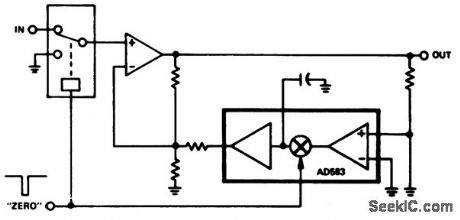
Sample-and-hold circuit used to automatically zero a high-gain amplifier (courtesy Analog Devices, Inc.). (View)
View full Circuit Diagram | Comments | Reading(566)
LOGIC_RESETTABLE
Published:2009/7/10 4:31:00 Author:May

DG200 CMOS analog switch serves for discharging integrator capacitor C rapidly for high logic input pulse, Other section of switch disconnects integrator from analog input when logic goes high. When logic input is returned to low, integrator is triggered. Diodes prevent capacitor from charging to over 15V.- Analog Switches and Their Applications, Siliconix, Santa Clara, CA, 1976, p 7-68. (View)
View full Circuit Diagram | Comments | Reading(648)
BASIC_MULTIVIBRATOR
Published:2009/7/10 4:31:00 Author:May


When this circuit is turned on, the natural offset of the devices serves as an automatic starting voltage.Assume that output voltage VO goes positive and the positive feedback through R2 and R1 forces the out-put to saturate. The high-voltage level at VO, then charges C through R3, until the voltage at the inverting input exceeds that at the noninverting input.As the inverting input exceeds the noninverting input level, the output switches to the negative saturation voltage. This action starts the capacitor discharging toward the new noninverting input level. When the capacitor reaches that level, the op amp switches back to the positive saturation voltage, and the process starts again. With the TL071, the positive and negative output levels are nearly equal, which results in a 50% duty cycle. The total time period of one cycle will be: (View)
View full Circuit Diagram | Comments | Reading(565)
DIGITAL_COMPASS
Published:2009/7/10 4:29:00 Author:May

A four output Hall sensor combined with a few logic gates produce this digltal compass. The NOR gates resolve the four Hall outputs into eight distinct compass directions. LEDs to indicate direction aredriven by eight inverters. A power supply for 5.25-to 18-Vdc operation IS shown in the figure. (View)
View full Circuit Diagram | Comments | Reading(1804)
LED_MILLIVOLTMETER
Published:2009/7/10 4:28:00 Author:May

This circuit uses a dc amplifier (324) in a bar-graph circuit that uses an LM339 Quad comparator IC to sense dc levels.The LEDs will light every 100 mV.The 324 op amp is configured to provide a gain of 100×to increase this sensitivity to 1 mV.Two auxiliary LEDs indicate power on and ×100 gam setting. (View)
View full Circuit Diagram | Comments | Reading(2559)
5V_AT_10A_WITH_CURRENT_LIMITING
Published:2009/7/19 20:13:00 Author:Jessie

Combination of three transistors and SN52105 or SN72305 regulator provides foldback current limiting for overload protection. Input voltage can be up to 40 V greater than 5-V output. Load regulation is about 0.1%, and input regulation is 0.1%/V.Regulators are interchangeable with LM105 and LM305 respectively.- The Linear and Interface Circuits Data Book for Design Engineers, Texas Instruments, Dallas, TX, 1973, p 5-9. (View)
View full Circuit Diagram | Comments | Reading(1685)
Sample_and_hold_circuit_with_Av_=___1
Published:2009/7/19 20:13:00 Author:Jessie

Sample-and-hold circuit with Av = + 1. The chip is an AD582 sample-and-hold amplifier (courtesy Analog Devices, Inc.). (View)
View full Circuit Diagram | Comments | Reading(620)
CURRENT_LOOP_SCR_CONTROL
Published:2009/7/10 4:27:00 Author:May

This circuit allows a 4-to 20-mA current loop to control an isolated SCR drive, IC1A and B are one-shots, Q2 detects zero crossings of the 120 Vac line, which trisaers one-shot IC1B. IC1A causes Q1 to discharge C2. When C2 recharges through Rz, it triggers IC1A, and the optoisolatoror and SCR1 /SCR2.Trig- gering of SCR1 and SCR2 is a function of input current, which can control motor speed, light intensity, etc. (View)
View full Circuit Diagram | Comments | Reading(1149)
DUAL_OUTPUTS_WITH_TRIMMING
Published:2009/7/19 20:10:00 Author:Jessie

Trimming pots connected across outputs provide positive or negative currents for producing small trimming voltages across 33-ohm ground-leg resistors of National regulators. Same components can be used for higher output voltages, but resistance values of pots should be increased if power dissipation becomes problem.-C. T. Nelson, Power Distribution and Regulation Can Be Simple, Cheap and Rugged, EDN Magazine, Feb. 20, 1973, p 52-58. (View)
View full Circuit Diagram | Comments | Reading(656)
Notch_filter_using_an_ECG947_dual_operational_amplifier_as_a_gyrator
Published:2009/7/19 20:10:00 Author:Jessie

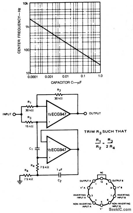
Notch filter using an ECG947 dual operational amplifier as a gyrator. The ECG947 is short-circuit protected and requires no external components for frequency compensation (courtesy GTE Sylvania Incorporated). (View)
View full Circuit Diagram | Comments | Reading(589)
LOW_COST_WITH_DISCRETE_ELEMENTS
Published:2009/7/19 20:09:00 Author:Jessie

Performance is comparable to that of combined discrete and monolithic circuits, with load regulation of 0.01%, line regulation of 0.05%, ripple rejection of 0.1%, and output ripple and noise of 1 mV. Output is 1 A at 5 V. Foldback short-circuit protection is provided by Tr4, with maximum current determined by value of R. C2, which can be 100 μF, gives extra ripple rejection by introducing more AC feedback into loop.TIP32A is plastic series transistor, and is not critical; many other types will work equally well.-K. W. Mitchell, High Performance Voltage Regulator, Wireless World, May 1976, p 83-84. (View)
View full Circuit Diagram | Comments | Reading(777)
| Pages:820/2234 At 20801802803804805806807808809810811812813814815816817818819820Under 20 |
Circuit Categories
power supply circuit
Amplifier Circuit
Basic Circuit
LED and Light Circuit
Sensor Circuit
Signal Processing
Electrical Equipment Circuit
Control Circuit
Remote Control Circuit
A/D-D/A Converter Circuit
Audio Circuit
Measuring and Test Circuit
Communication Circuit
Computer-Related Circuit
555 Circuit
Automotive Circuit
Repairing Circuit