
Circuit Diagram
Index 821
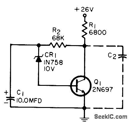
RIPPLE_PREAMP_SUPPLY
Published:2009/7/19 20:07:00 Author:Jessie

Shunt regulator re-moves virtually all AC line ripple without using large capacitor, making it ideal for audio applications where freedom from ripple is more important than precise supply voltage level. Circuit cannot be damaged by short-circuits. Tr3 may be power transistor or Darlington.-P. S. Bright, Ripple Eliminator, Wireless World, April 1977, p 62.
(View)
View full Circuit Diagram | Comments | Reading(805)
ANALOG_START_STOP_AND_RESET
Published:2009/7/10 4:26:00 Author:May

One section of DG300 dual analog switch serves for discharging integrator capacitor C through RL when resetting integrator, with start/stop switch section being held open by control logic.When both switches are open, output of integrator is held.- Analog Switches and Their Applications, Siliconix, Santa Clara, CA, 1976, p7-81. (View)
View full Circuit Diagram | Comments | Reading(1965)
_10_TO__25V_AT_100mA
Published:2009/7/19 20:04:00 Author:Jessie

Series regulator uses opamp as differential amplifier and extra transistor Q2 as current limiter. When 100 mA is drawn, 0.6 V is developed across R2 to make Q2 conduct, pulling al base in negative direction. This action prevents excessive current from being passed by Q1.-H. Olson, Power-Supply Servicing, Ham Radio, Nov. 1976, p 44-50. (View)
View full Circuit Diagram | Comments | Reading(842)
0_15V_AT_2A
Published:2009/7/19 19:57:00 Author:Jessie

Basic zener-opamp regulator output of 6.6V is scaled up to maximum of 15 V, adjusted with R4, by adding buffer opamp A2, and current-hoosting transistors. Q2 provides short-circuit protection by sensing load current through R7. Large output capacitor C1, maintains low output impedance at high frequencies where gain of A2, falls off.-W. G. Jung, IC 0p-Amp Cookbook, Howard W. Sams, Indianapolis, IN, 1974, p 158-159. (View)
View full Circuit Diagram | Comments | Reading(818)
CONTINUITY_TESTER
Published:2009/7/10 4:23:00 Author:May

Using a comparator, this continuity tester applies only about 300mV to the circuit to be tested. This avoids false readings in semiconductor circuits. (View)
View full Circuit Diagram | Comments | Reading(0)
01_24V_AT_1A
Published:2009/7/19 19:55:00 Author:Jessie
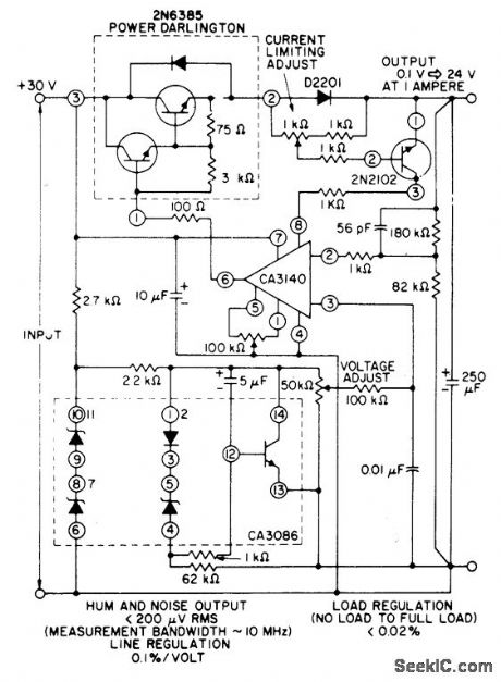
High4mpedance reference-voltage divider across 30-V supply serves CA3140 connected as noninverting power opamp with gain of 3.2. 8-V reference input gives maximum output voltage of about 25V. D2201 high-speed diode serves as current sensor for 2N2102 current-limit sensing amplifier. Current-limiting point can be adjusted over range of 10 mA to 1 A with single 1k pot. Power Darlington serves as series-pass element.- Linear Integrated Circuits and MOS/FET's, RCA Solid State Division, Somerville, NJ, 1977, p 248-256. (View)
View full Circuit Diagram | Comments | Reading(1646)
ZENER_NOISE_GENERATOR
Published:2009/7/17 23:05:00 Author:Jessie
Amplifies noise voltage developed across conducting zener diode. Zener current is fed to base of transistor, which has nominal current gain of 75.-G. Richwell, One-Stage Semiconductor Noise Generator, EEE, 12:7, p 26-28. (View)
View full Circuit Diagram | Comments | Reading(1802)
RMS_CONVERTER
Published:2009/7/10 4:23:00 Author:May


Converts analog voltage to RMS equivalent by squaring operation followed by integration and squarerooting. Bipolar input signal is first converted into linear absolute value with Optical Electronics 9004 absolutevalue module, as required for processing by 5904 unipolar devices. Pots are used to establish 10-V full-scale level.R1C1is integration time constant.- Simple RMS Converter, Optical Electronics, Tucson, AZ, Application Tip 10246. (View)
View full Circuit Diagram | Comments | Reading(874)
BACKGROUND_NOISE_SUPPRESSOR
Published:2009/7/17 23:04:00 Author:Jessie

With control set for maximum resistance, only desired a-c voltage peaks above 4.5 V are passed by diodes. Balanced variable-thresh-old circuit achieves this suppression of weak background noise without affecting a-c balance of signals.-W. E. Earle, A-C Threshold Converts to Switch, Electronics, 31;1, p 96-99. (View)
View full Circuit Diagram | Comments | Reading(1023)
SIMPLE_VARIABLE_FREQUENCY_SQUARE_WAVE_GENERATOR
Published:2009/7/10 4:23:00 Author:May

A CD4046B PLL is used as a simple generator.The range is 200 Hz to 2 kHz, but it can be changed by changing C1. (View)
View full Circuit Diagram | Comments | Reading(1465)
4_DECADE_SQUARE_WAVE_GENERATOR
Published:2009/7/10 4:21:00 Author:May

This circuit will generate a square wave of 2 Hz to 20 kHz. The circuit uses an op amp in a relaxation-oscillator configuration. The output is about 15 VPP. R1 through.R4. are calibrols for the four frequency ranges, as selected by S1-a and 51-b. R10 adjusts the output level. (View)
View full Circuit Diagram | Comments | Reading(737)
AC_COUPLED_JFET_
Published:2009/7/10 4:19:00 Author:May

Use of C1 as Miller integrator or capacitance multiplier allows simple circuit to handle very long time constant while providing high voltage gain. Circuit also offers low distortion with low noise and high dynamic range.- FET Databook, National Semiconductor, Santa Clara, CA, 1977, p 6-26. (View)
View full Circuit Diagram | Comments | Reading(917)
GATE_CAPACITOR_PROTECTS_SCS_AGAINSTRFI
Published:2009/7/17 23:03:00 Author:Jessie

Capacitor between gate and cathode provides shunt path at higher frequencies to prevent firing of silicon controlled switch by r-f interference. Values in circuit will give protection from 32-V signals between 100 kc and 30 Mc. –R. J. Sanford, Can RFI Control Prevent Weapons Failures?, Electronics, 36:45, p 43-45. (View)
View full Circuit Diagram | Comments | Reading(488)
SOUND_METER_RECTIFIER
Published:2009/7/17 23:02:00 Author:Jessie
Used with sound level meter to provide indication proportional to rms value of wideband noise, in two-segment linear approximation to required square-law characteristic.-W. V. Richings and B. J. White, Transistorized Sound Level Meter, Electronics, 33:25, p 64-66. (View)
View full Circuit Diagram | Comments | Reading(1212)
SQUELCH_FOR_MOBILE
Published:2009/7/17 23:02:00 Author:Jessie
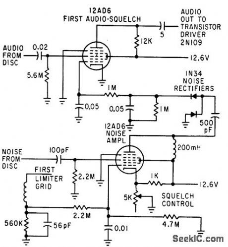
Reduces background noise, to prevent operator fatigue during no-signal periods. Double-action squelch is obtained by using negative voltoge at first limiter grid during signal periods to cut off 12AD6 noise amplifier.-C. Gonzalez and R. J. Nelson, Design of Mobile Receivers with Low-Plate-Potential Tubes, Electronics, 33:34, p 62-65. (View)
View full Circuit Diagram | Comments | Reading(1110)
SQUELCH_FOR_DOUBLE_SUPERHET
Published:2009/7/17 22:42:00 Author:Jessie
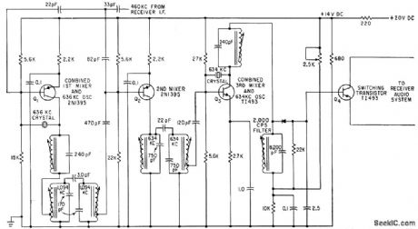
Carrieroperated squelch level is automatically adjusted to best compromise for incoming signal. Squelch can be adjusted to open on 0.5-microvolt input signal while remaining closed when subject to full output of noise generator-J. M. Tewksbury, Receiver Squelch Control Uses Double Superheterodyne, Electronics, 35:3, p 44-46. (View)
View full Circuit Diagram | Comments | Reading(1611)
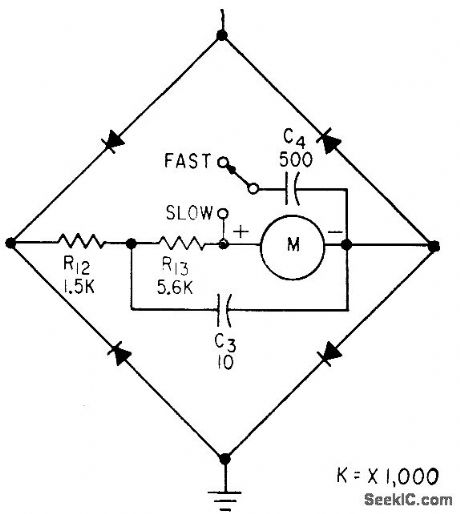
SCR_NOISE_SUPPRESSOR
Published:2009/7/17 22:40:00 Author:Jessie
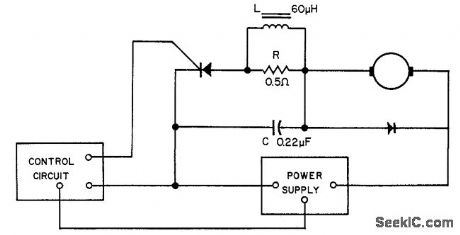
Used to suppress circuit noise generated when scr is switched on, without materially affecting power-handling capacity or efficiency. Load shown is d-c series motor.-Noise Reducer for SCR, EEE, 10:10, p 94. (View)
View full Circuit Diagram | Comments | Reading(1124)
A_F_AMPLIFIER_WITH_SQUELCH_2
Published:2009/7/17 22:40:00 Author:Jessie
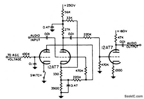
Used to make first audio stage inoperative during no-signal condition in communication receiver.-NBS, Handbook Preferred Circuits Navy Aeronautical Electronic Equipment, Vol. 1, Electron Tube Circuits, 1963, p N12-2. (View)
View full Circuit Diagram | Comments | Reading(660)
A_F_AMPLIFIER_WITH_SQUELCH_1
Published:2009/7/17 22:39:00 Author:Jessie

Input is obained from noise rectifier and amplifier of communication receiver. Squelch is used to make first audio stage inoperative during no-signal condition.-NBS, Handbook Preferred Circuits Navy Aeronautical Electronic Equipment, Vol, 1, Electron Tube Circuits, 1963, p N12-2. (View)
View full Circuit Diagram | Comments | Reading(684)
SOUND_LEVEL_METER
Published:2009/7/17 22:26:00 Author:Jessie

Two-transistor circuit takes high-impedance microphone feeding compound grounded-collector stage in which collector, emitter load, and biased resistor of Q1 are bootstrapped.-W. V Richings and B. J. White, Transistorized Sound Level Meter, Electronic, 33:25, p 64-66. (View)
View full Circuit Diagram | Comments | Reading(4940)
| Pages:821/2234 At 20821822823824825826827828829830831832833834835836837838839840Under 20 |
Circuit Categories
power supply circuit
Amplifier Circuit
Basic Circuit
LED and Light Circuit
Sensor Circuit
Signal Processing
Electrical Equipment Circuit
Control Circuit
Remote Control Circuit
A/D-D/A Converter Circuit
Audio Circuit
Measuring and Test Circuit
Communication Circuit
Computer-Related Circuit
555 Circuit
Automotive Circuit
Repairing Circuit