
Circuit Diagram
Index 503
LT3436EFE high-power white LED driver circuit diagram
Published:2011/9/6 4:29:00 Author:Lucas | Keyword: high-power white LED, driver
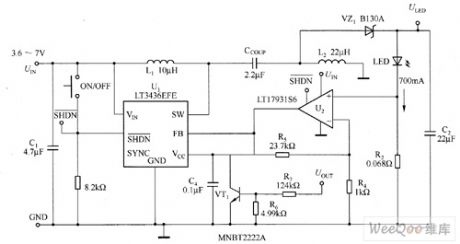
The SEPIC power white LED driver circuit with wide input voltage composed of LT3436EFE is shown as the figure, and in the wide input voltage range (3.6 ~ 7V), it can provide 700mA driver current for the LuxeonV series of white LEDs. Converter's output voltage is 6.8V, which is the LED (Model LXHL-LW6C)'s forward voltage. U1 is the high-efficient, 3A thermally enhanced LT3436EFE on-board power switch, which can simplify the regulator design and layout. It also gives the white LED driver sufficient current without overheating. U2 is the LTl7931S6 op amp with SOT-2 package.
(View)
View full Circuit Diagram | Comments | Reading(1677)
NCP5010 white LED driver circuit
Published:2011/8/29 2:37:00 Author:Lucas | Keyword: white LED driver
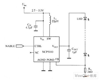
The IC integrates the rectification function, and it can provide 22V voltage, and the single resistor can be used to set the white LED current, and output power is up to 500mW, and it can drive 2 to 5 series of white LEDs. NCP5010 input voltage range is 2.7 ~ 5.5V, and the input efficiency can be up to 84% at 4.2V and 30mA, and the cut off current is 1μA with real cut, short-circuit and overvoltage protection, undervoltage cut off. In addition, due to its pulse width modulation (PWM) boost converter frequency is 1MHz, it integrates the Schottky rectifier.
(View)
View full Circuit Diagram | Comments | Reading(737)
MAX1582 LED driver circuit diagram
Published:2011/8/31 20:28:00 Author:Lucas | Keyword: LED driver
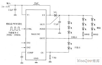
For wireless handheld devices with color display, white LED backlighting is the main backlight. White LED backlight has the features of simple circuit, high efficiency, high reliability. New generation of mobile phones generally use 3 to 4 white LEDs as the main display backlight; it uses two white LEDs for the sub-display (folding design) backlight; it uses six or more white / color LEDs for the keyboard backlight. If mobile phones integrates with cameras, it also needs at least four white LEDs for flashing, MPEG video sources. Thus, a mobile phone uses 16 white LEDs in a total.
(View)
View full Circuit Diagram | Comments | Reading(1863)
MAX16821/MAX16821A/MAX16821B/MAX16821C white LED driver circuit diagram
Published:2011/8/25 21:23:00 Author:Lucas | Keyword: white LED driver
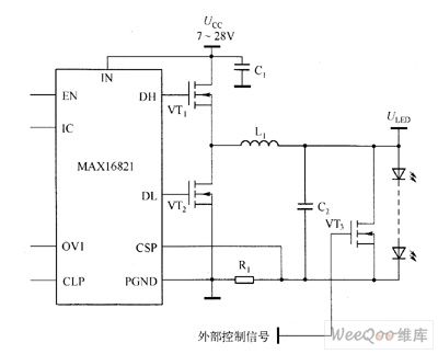
MAX16821A/MAX16821B/MAX16821C's main technical characteristics are as follow. ① 30A output current. ② it uses the average current mode control, true differential remote output detection technology. ③ 125kHz ~ 1.5MHz Programmable / synchronized switching frequency. ④ 4.75 ~ 5.5V or 7 ~ 28V input voltage range. ⑤ 0.1V/0.03V two kinds of white LED current-sense options, which allow the maximum efficiency (MAX16821B/MAX16821C). ⑥ it has no-lockout overvoltage protection output and thermal shutdown protection. ⑦ Integrated 4A Gate Driver. ⑧ low-buck mode, which can be chosen in two structures with synchronous rectification or not.
(View)
View full Circuit Diagram | Comments | Reading(899)
MAX6946/MAX6947 white LED driver circuit diagram
Published:2011/8/25 21:30:00 Author:Lucas | Keyword: white LED driver
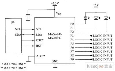
MAX6946/AX6947's main technical characteristics are as follow. ① 400kbps, 6V withstand voltage, I2C/SMBus-compatible serial interface. ② working voltage is 2.25 ~ 3.6V. ③ when the power is turned on, I / O port is implied in high impedance (it can be synchronized with the turning off of LED) state. ④ I / O port has the 7V overvoltage protection. ⑤ I / O port output type: open-drain output or open-drain logic output when voltage rating is 7V (10mA or 20mA static / PWM output can be synchronized with the LED constant current driver). ⑥ I / O ports support hot insertion. ⑦ each LED can be synchronized with the separate 8-bit PWM brightness control.
(View)
View full Circuit Diagram | Comments | Reading(851)
LT3474 White LED driver circuit diagram
Published:2011/8/29 3:00:00 Author:Lucas | Keyword: White LED driver
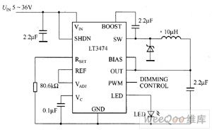
LT3474 is the step-down DC / DC converter with fixed frequency, the LED driver circuit composed of LT3474 is shown in Figure 3-58. Its internal sense resistor is mainly used to monitor the output current in order to achieve stable and accurate flowing. The device is ideal for driving high current white LED, and it can maintain high output current accuracy in 35mA ~ 1A wide current range in order to achieve a wide dimming range. The dimming range can use PWM pin and an external N-channel MOSFET to further expand and achieve 1000:1 dimming range. LT3474's switching frequency can be programmed in the range of 200kHz ~ 2MHz.
(View)
View full Circuit Diagram | Comments | Reading(1057)
MAX6966/MAX6967 white LED driver circuit diagram
Published:2011/8/25 21:34:00 Author:Lucas | Keyword: white LED driver
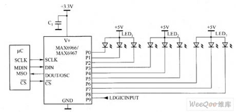
MAX6966's main technical characteristics are as follow. ① it has high-speed 26MHz SPI / QSPI / MICROWIRE compatible serial port. ② 2.25 ~ 3.6V operating voltage. ③ when the power is turned on, I / O port is implied to high impedance (LED turns off) state. ④ I / O port input over-voltage protection value is 7V. ⑤ it has open-drain output when I / O port output rated voltage is 7V. ⑥ I / O port output is 10mA or 20mA constant current, static / PWM or open-drain logic output. ⑦ I / O ports support hot insertion. ⑧ each outputs independent 8-bit PWM control. ⑨ it has Schmitt logic input with overvoltage protection.
(View)
View full Circuit Diagram | Comments | Reading(1562)
MAX7302 White LED driver circuit diagram
Published:2011/8/25 20:51:00 Author:Lucas | Keyword: White LED driver

MAX7302's main technical characteristics are as follow. ① 1.62 ~ 5.5V I / O port level conversion power (ULA). ② Power supply voltage is 1.62 ~ 3.6V. ③ 9-way independent configured GPIO ports. ④ 25mA (max) port outputs sink current (the maximum ground current is 100mA). ⑤ The independent 11-stage PWM brightness control with 15-stage flash output control in output end, and 1kHz PWM cycle provides a flicker-free white LED brightness control. ⑥ Input overvoltage protection is up to 5.5V (ULA). ⑦ oscillator input and output can cascade multiple devices. ⑧ I / O port can be configured as logic gates (CLA).
(View)
View full Circuit Diagram | Comments | Reading(869)
Schematic diagram of clock circuit composed of AT89C2051
Published:2011/9/7 4:15:00 Author:Vicky | Keyword: schematic diagram, clock circuit

The circuit composition determines that the LED adopts anodic Nixie tube. It can use LQ5101BS general luminous diode and the driving triode can use 2SA1015 or 2SC1815 types which is easy to gain. Of cause, the triode can also use low-power triode such as S9012, S9013,S9014,2N5401,and 2N5555 etc. There are no special requirements for other components. To make the experiment easier, monolithic AT89C2051 can use DIP20P socket. The program need no debugging after written, and it can be copied to AT89C2051. What worth mentioning is that AT89C2051 is a flash program memorizer, and the program can be rewritten repeatedly, which makes it very easy to conduct experiments. (View)
View full Circuit Diagram | Comments | Reading(8628)
Grain Moisture Tester
Published:2011/9/3 22:39:00 Author:Ariel Wang | Keyword: Grain, Moisture

A, B are two measuring electrodes. As the resistance value of food is generally high.Even during the measurement electrode with high voltage of about 150V, the current between two electrodes is only less than 1μA.The value of the measurement should be amplified by IC1 Integrated operational amplifier 5G3140 and then it could be indicated by header M. The higher the grain moisture content, the greater the current between the electrodes A and B , the greater the value the meter indicates. The pulse oscillator is made up of IC2's Time-base circuit 555.It is stepped up by transformer T,commutated by the diode.Then it generates 150V high voltage for the measurement of the electrodes.
(View)
View full Circuit Diagram | Comments | Reading(3335)
Circuit diagram of power line carrier communication IC-LM1893 and its application
Published:2011/9/7 4:18:00 Author:Vicky | Keyword: power line carrier communication
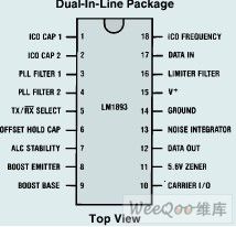
LM1893 is a power line carrier communication integrated circuit developed by National Semiconductor. It contains the whole functions of sending and receiving data. It can realize half duplex communication of serial data. It only needs few exterior components to constitute and whole power line carrier communication system, which is applicable in industrial automatic control system, building data or voice communication, house-application central control, emergency call box system in hospital, fire proofing annunciator and computer data transmitting and so on. Its main features are as follows:
FSK anti-noise modulation technology
Pulse generator with alternative noise filtering
Data transmitting rate :up to 4.8KB
Sine wave carrier frequency to reduce radio frequency disturbance
Radio frequency rate which can be 10 times stronger
Alternative carrier frequency between 50 and 200kHz
Compatible TTL and MOS logic level
Adjustable voltage, power and level
Ability to drive all sorts of level
LM1893 working principle
(View)
View full Circuit Diagram | Comments | Reading(6497)
Deep-current negative feedback differential motion amplifier diagram
Published:2011/9/7 4:19:00 Author:Vicky | Keyword: deep-current, negative feedback, differential motion amplifier

Deep-current negative feedback differential motion amplifier diagram
(View)
View full Circuit Diagram | Comments | Reading(836)
The electronic voltmeter of LED display
Published:2011/9/2 3:00:00 Author:Ariel Wang | Keyword: electronic , LED display

The circuit consists of 6 LEDs,two integrated circuits and some resistors.It could display the storage battery's voltage value of the motors,cars and electric bicycles .It is very convenient to use.
(View)
View full Circuit Diagram | Comments | Reading(639)
Remote control coding chip RT1517
Published:2011/9/7 4:26:00 Author:Vicky | Keyword: Remote control coding chip, remote control IC

It’s a learning-code coding chip RT1517 and decoding chip for receiving
Security
1,6 million group coder
Standard 40 remote control units for learning and memorizing
Using learning-code technology
Good fault-tolerant ability
Operation
2.0 – 5.5 operating voltage
Low power dissipation
Learn-LED pin learning output indication
Auto modulation for Baud rate
Other features
Few exterior components
Being used as individual decoder
Easy to produce and no need of coding in PCB
Typical application
Auto multimedia central control system
Auto/Moto Annunciator
House security
Auto electronic lock and garage gate
Identity resolution
Anti-theft system (View)
View full Circuit Diagram | Comments | Reading(1379)
Electromagnetism speed measurement control circuit diagram
Published:2011/9/7 4:29:00 Author:Vicky | Keyword: Electromagnetism speed measurement control circuit

Electromagnetism speed measurement control circuit diagram (View)
View full Circuit Diagram | Comments | Reading(1146)
ZCS PWM DC/DC converter circuit diagram
Published:2011/9/7 4:08:00 Author:Vicky | Keyword: ZCS PWM DC/DC converter


Topological structure: Buck DC/DC ZCS PWM converter, main switch T1 (including antiparallel diode D1), booster diode T2 (D2 is the antiparallel diode of T2).
Suppose thatthe diode switches are all ideal devices; the inductances and capacitances are all ideal components; Cr is big enough, Lf is also big enough, and Lf>>Lr. I switching cycle, output voltage is 0, remaining and unchanged; if it retains Io, unchanged, so Lf, Cf and load resistance can be regarded as a constant current source Io.
The state of switch: In a switching cycle Ts, converter has 5 switching state. Every switching state has a corresponding equivalence circuit. (View)
View full Circuit Diagram | Comments | Reading(2902)
Circuit diagram of 9V charger which can preset the end voltage of charging
Published:2011/9/7 4:00:00 Author:Vicky | Keyword: 9V charger, preset the end voltage of charging
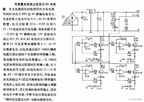
The picture is a circuit of 9V charger which can preset the end voltage of charging. The charger has four groups of identical charging circuit, which can charge four pieces of PP3 type 9V nickel-cadmium battery at the same time. The end voltage can be set between 8.5 to 10V. The voltage comparators IC2A~IC2D constitute four groups of charging circuit with T1~T4 respectively. Every circuit can charge a PP3 type 9V nickel-cadmium battery. 15V DC voltage is divided by voltage divider composed of R17, P1, R18, and D1. The base voltage of 8.5~10V can be gained in the sliding end by adjusting P1. The voltage is added to non-inverting input ends of the four comparators by four 100KΩ isolation resistance. The voltage of every group charged is added to inverting end of its corresponding comparators via a 100KΩ resistance to compare with the base voltage. (View)
View full Circuit Diagram | Comments | Reading(1978)
Express charger circuit diagram
Published:2011/9/7 3:58:00 Author:Vicky | Keyword: Express charger circuit
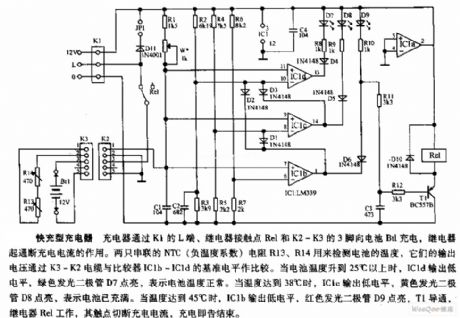
Express charger circuit diagram
The charger charges Bt1via the Lend of K1, contact point Rel of relay, and pin 3 of K2-K3, while the relay acts to control on-off of the charging current. Two NTC (negative temperature coefficient) resistances R13 and R14 in serial are used to examine the temperature of battery. Their output voltage compares with the base level of comparators IC1b ~IC1d via wire cable K3 ~ K2. When the battery temperature rises to above 25℃, IC1d outputs low level, and the green luminous diode D7 is lighted to show that the battery temperature is normal. When the temperature rises to 38℃, IC1c outputs low level, and yellow luminous diode D8 is lighted to show that the battery is full charged. When the temperature rises to 45℃, IC1b outputs low level, the red luminous diode D9 is lighted, T1 is conducted, relay Rel starts working with its contact point cutting off the charging current, and the charging ends. (View)
View full Circuit Diagram | Comments | Reading(1328)
The home points electrotherapy
Published:2011/9/3 23:48:00 Author:Ariel Wang | Keyword: home , points

There are many different types of electronic treatment in the medical device market.They are said that they have a special effect to certain diseases.The price is also not cheap. In fact, most of them are nothing more than some electronic treatment devices which can output some pulses .They may have the effect to some diseases in accordance with different frequencies of the output pulse waveform.It is the home points electrotherapy shown as the chart. The whole circuit is mainly composed of a Schmitt trigger CD40106 six.The ultra-low-frequency multivibrator oscillation consists of the Dl, Rl, VDl and C1. The oscillation frequency is 0.5 ~ 5Hz. It is regulated by RPl.
(View)
View full Circuit Diagram | Comments | Reading(1775)
Regulator DC-DC Circuit and Pin of Power Supply Monitor and its Main Features TA7501S Amplified Circuit
Published:2011/9/6 2:57:00 Author:Zoey | Keyword: Regulator, DC-DC Circuit, Pin of Power Supply Monitor, Amplified Circuit

TA7501S Amplified Circuit controlled by Leakage Current
The circuit that can be cut off by high-speed leakage current is available for leakage cutters,which have a sensitivity of 15mA. The typical value of trip voltage is 7mV and it will turn to be 1ms when it increases. The maximum current of the power supply is 10mA and the power is 400mW. The working temperature is between -40 ℃to +85℃. The lock circuit itself has an interior voltage stabilizing circuit and an interior SCR rectifier that can conduct externally. (View)
View full Circuit Diagram | Comments | Reading(681)
| Pages:503/2234 At 20501502503504505506507508509510511512513514515516517518519520Under 20 |
Circuit Categories
power supply circuit
Amplifier Circuit
Basic Circuit
LED and Light Circuit
Sensor Circuit
Signal Processing
Electrical Equipment Circuit
Control Circuit
Remote Control Circuit
A/D-D/A Converter Circuit
Audio Circuit
Measuring and Test Circuit
Communication Circuit
Computer-Related Circuit
555 Circuit
Automotive Circuit
Repairing Circuit