
Circuit Diagram
Index 519
Three-capacitor|braking circuit
Published:2011/8/30 2:59:00 Author:Christina | Keyword: Three-capacitor braking circuit

View full Circuit Diagram | Comments | Reading(722)
Samsung CE959 microwave circuit
Published:2011/8/30 3:01:00 Author:Christina | Keyword: Samsung, microwave
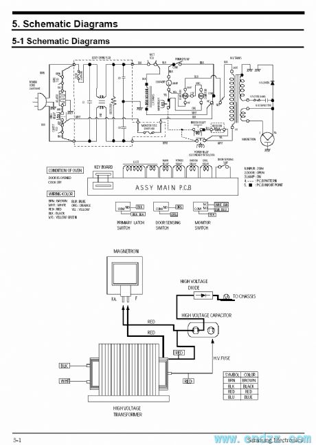

View full Circuit Diagram | Comments | Reading(1398)
Three-phase exhaust fan electricity saving automatic control circuit
Published:2011/8/30 3:07:00 Author:Christina | Keyword: Three-phase, exhaust fan, electricity saving, automatic control

In some poorly ventilated place, the long-term operation of the exhaust fan will waste the electricity, and the exhaust fan is easy to burn out. The circuit of the figure can achieve the automatic stop of the exhaust fan M, also the automatic start of the exhaust fan M. The interval time is set by the potentiometers RP1 and RP2.
(View)
View full Circuit Diagram | Comments | Reading(2172)
The RF wide band amplifier unit circuit of separated elements
Published:2011/8/23 22:13:00 Author:Borg | Keyword: wide band amplifier, separated elements

The RF wide band amplifier unit circuit of separated elements is shown as above.
(View)
View full Circuit Diagram | Comments | Reading(1106)
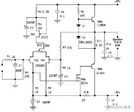
The self-made independent element 50W hi-fi power amplifier circuit
Published:2011/8/23 22:13:00 Author:Borg | Keyword: independent element, hi-fi, power amplifier

The power amplifier stage of the amplifier circuit consists of the compensatory tube emitter follower, the backward feedback of the big circuit makes the drive compensatory tube signal in the linear range. The circuit makes sure the 2 tubes conduct in different time in the structure, so the power supply won't be short.
Ideal transistors can conduct or block quickly, however, triodes switch speed is limited, not to say the large power tube. When the changing signal which is put in the tube is reversed, the 2 tubes may be conducting at the same time. (View)
View full Circuit Diagram | Comments | Reading(3930)
The 30W single terminal audio power amplifier circuit of type A
Published:2011/8/23 22:13:00 Author:Borg | Keyword: single terminal, audio power amplifier
The 30W single terminal audio power amplifier circuit of type A is shown as above.
(View)
View full Circuit Diagram | Comments | Reading(3235)
The domestic experiment electro medical apparatus circuit
Published:2011/8/23 22:13:00 Author:Borg | Keyword: domestic, electro medical apparatus
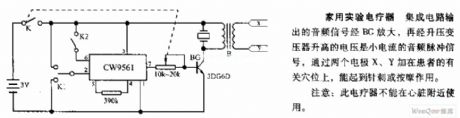
The domestic experiment electro medical apparatus circuit The audio signal output by the integrated circuit is amplified by BG, and the voltage boosted by the transformer is the audio pulse signal of the small current, by putting the two electrodes of X and Y on the acupuncture points of the patients, the machine can fulfill the function of puncturing or massage.Notes: the electro medical apparatus can't be used near the heart.
(View)
View full Circuit Diagram | Comments | Reading(1377)
The muscle stretch tester circuit
Published:2011/8/23 22:14:00 Author:Borg | Keyword: muscle stretch tester
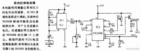
The circuit modulates 555 multi-resonance by using the capacitance sensor that measures movement and pressure, the frequency is tested out by the NE560B PLL integrated circuit, and it generates the DC output voltage. The sensor zero frequency can be tested out by the 12-pin of NE560B. The VCO (voltage control oscillator) frequency of the PLL circuit should be tested out from the 2N3393 emitter which connects with 5-pin.
(View)
View full Circuit Diagram | Comments | Reading(701)
The amplifier pin and main features--the XR4202 4-line calculator and silent low-power op-amp
Published:2011/8/25 4:03:00 Author:Borg | Keyword: amplifier pin, calculator, op-amp

the XR4202 4-line calculator and silent low-power op-ampThe input offset voltage is 1mV; the biased current is 80nA; the gain band width GB=3.5MHz; the converting ratio is 1.6V/μs; the differential mode input voltage is ±30V; the common mode input voltage is ±30V; the power consumption is 550mW; the static power consumption 50mW.
(View)
View full Circuit Diagram | Comments | Reading(655)
The amplifier pin and main features--XR4202 programmable 4-line calculator
Published:2011/8/25 3:57:00 Author:Borg | Keyword: amplifier pin, calculator

XR4202 programmable 4-line calculatorThe input offset voltage is 2mV; the gain band width is GB=3.5MHz; the converting ratio is 1.5V/μs; the noise is 25nV/(1KHz); the consumption current is 1.7mA; the power supply voltage is ±18V; the differential mode input voltage is ±30V; the power consumption is 550mW.
(View)
View full Circuit Diagram | Comments | Reading(620)
The amplifier pin and main features--the TL322 op-amp of dual-single power supply
Published:2011/8/25 3:51:00 Author:Borg | Keyword: amplifier pin, op-amp, dual-single power supply

The TL322 op-amp of dual-single power supply The input offset voltage is 2mV; the temperature drift is 10μV/℃; the biased current is 200nA; the gain band width is 1MHz; the converting ratio is 600V/μs; the consumed current is 1.4mA; the voltage of the power supply is ±1.5~±18V, it can work with a single power supply; the differential mode input voltage is ±36V; the common mode input voltage is ±18V; its output stage is divided into 2 types which are A and B; its power consumption is (JG0825mW/(P)1000mW).
(View)
View full Circuit Diagram | Comments | Reading(643)
The amplifier pin and main features--the TL321 op-amp of single power
Published:2011/8/25 3:39:00 Author:Borg | Keyword: amplifier pin, op-amp

TL321--the single power supply op-ampThe input offset voltage is 2mV; the biased current is 40nA; the consuming current is 400μA; the voltage of the power supply is ±1.5~±16V, it can work with a single power supply; the input voltage is -0.3~+32V.
(View)
View full Circuit Diagram | Comments | Reading(894)
The amplifier pin and main features--the general JEFT input op-amp of TL081
Published:2011/8/25 1:04:00 Author:Borg | Keyword: amplifier pin, general JEFT, input op-amp

TL081/TL082/TL084--the general JFET input op-ampThe input offset voltage is 3mV; the temperature drift is 10μV/℃; the input bias current is 5pA; the gain band width is GB=3MHz; the converting speed rate is 13V/μs; the noise is 25nV/(1KHz); the consumed current is 1.4mA/(TL081), 2.8mA(TL082), 5.6mA(TL084); the power supply is ±18V; the differential mode input voltage is ±15V; the power consumption is 680mW. The approximate types are μPC4081, μPC4082 and μPC4084.
(View)
View full Circuit Diagram | Comments | Reading(2245)
The amplifier pin and main features--the TL136 op-amp of 4 high functions
Published:2011/8/25 1:16:00 Author:Borg | Keyword: amplifier pin, op-amp

TL136--the TL136 op-amp of 4 high functionsThe input offset voltage is 500μV; the biased current is 40nA; the gain band width is GB=3MHz; the converting speed rate is 2V/μs; the noise is 7.5nV/(1KHz); the consumed current is 5mA; the power supply voltage is ±15V; the power consumption is 800mW.
(View)
View full Circuit Diagram | Comments | Reading(605)
The amplifier pin and main features--the single power supply JEFT input op-amp of TL091
Published:2011/8/25 1:11:00 Author:Borg | Keyword: amplifier pin, general JEFT, input op-amp

TL091/TL092/TL094--the single power supply JEFT input op-ampThe input offset voltage is 5mV; the temperature drift is 10μV/℃; the input bias current is 200pA; the gain band width is GB=1MHz; the converting speed rate is 600mV/μs; the noise is 34nV/(1KHz); the consumed current is 1.5mA/(TL081), 3mA(TL082), 6mA(TL084); the power supply is ±1.5~±18V; it can work with a single power supply; the differential mode input voltage is ±36V; the common mode input voltage is ±18V; the power consumptions are (J)1025mW and (N)1150mW.
(View)
View full Circuit Diagram | Comments | Reading(1484)
The amplifier pin and main features--the general JEFT input op-amp of TL080/A
Published:2011/8/25 0:57:00 Author:Borg | Keyword: amplifier pin, JEFT, input op-amp

TL080/A--the general JEFT input op-ampThe input offset voltage is 3mV; the temperature drift is 10μV/℃; the input bias current is 5pA; the gain band width is GB=3MHz; the converting speed rate is 13V/μs; the noise is 25nV/(1KHz); the consumed current is 1.4mA; the power supply is ±18V; the differential mode input voltage is ±30V; the common mode input voltage is ±15V; the power consumption is 680mW.
(View)
View full Circuit Diagram | Comments | Reading(710)
The amplifier pin and main features--JEFT input op-amp of TL071
Published:2011/8/25 0:58:00 Author:Borg | Keyword: amplifier pin, op-amp, JEFT

TL071/TL072/TL074--the JFET input op-ampThe input offset voltage is 3mV; the temperature drift is 10μV/℃; the biased current is 5pA; the gain band width is GB=3MHz; the converting speed rate is 13V/μs; the noise is 18nV/(1KHz); the consumed current is 1.4mA/(TL071), 2.8mA(TL072), 5.6mA(TL074); the power supply is ±18V; the differential mode input voltage is ±30V; the common mode input voltage is ±15V; the power consumption is 680mW.
(View)
View full Circuit Diagram | Comments | Reading(2466)
Three electromotors sequence-start reversed order stop circuit
Published:2011/8/30 20:28:00 Author:Christina | Keyword: Three electromotors, sequence-start, reversed order, stop circuit

Some technological processes need the three electromotors, the sequence-start order is M1, M2, M3, the reversed order is M3, M2, M1. In this circuit, the normally open contact point of KM1 is connected into the control loop of KM2; the normally open contact point is connected into the control loop of KM3, if the KM1 will not close, the electromotor M1 is not the first start one, so the electromotor M2 can not start; also the M3, this is the sequence start. The reason of the reversed order stop is that the normally open auxiliary contact point of KM3 is connected with the two ends of the stop button STP2, the normally open auxiliary contact point of KM2 is connected with the two ends of the stop button STP1.
(View)
View full Circuit Diagram | Comments | Reading(3168)
The main features of the amplifier pin signal--TL066/A/B programmable JFET input op-amp
Published:2011/8/23 22:14:00 Author:Borg | Keyword: amplifier, programmable JFET, input op-amp

TL066/A/BprogrammableJFETinputop-amp
Input distortion voltage is 3mV; temperature drift is 10μV/⁰C; input distortion current is 30pA; gain band width is GB=1MHz; converting speed rate is 3.5V/μs; the noise 42nV/√Hz(1kHz); the current consumption is 200μA; ±1.2~±18V power supply; the differential mode input voltage is ±30V; the common mode input voltage ±15V; the power consumption is 680mW; the current of the changeable power supply is 5~200mA.
(View)
View full Circuit Diagram | Comments | Reading(897)
The main features of the amplifier pin--OPA633 buffering amplifier
Published:2011/8/23 22:14:00 Author:Borg | Keyword: amplifier pin, buffering amplifier
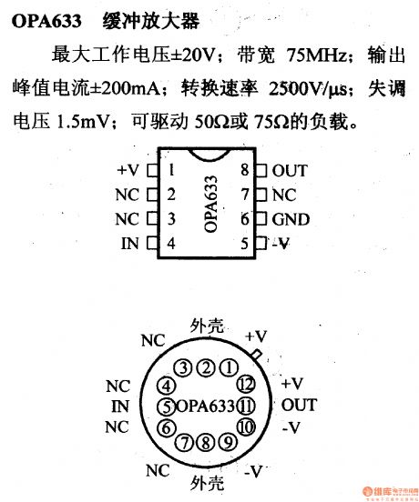
OPA633 buffering amplifier The maximum working voltage is ±20V; band width is 75MHz; output peak current is ±200mA; switching efficiency is 2500V/μS; the distortion voltage is 1.5mA; it can drive the load of 50Ω or 75Ω.
(View)
View full Circuit Diagram | Comments | Reading(763)
| Pages:519/2234 At 20501502503504505506507508509510511512513514515516517518519520Under 20 |
Circuit Categories
power supply circuit
Amplifier Circuit
Basic Circuit
LED and Light Circuit
Sensor Circuit
Signal Processing
Electrical Equipment Circuit
Control Circuit
Remote Control Circuit
A/D-D/A Converter Circuit
Audio Circuit
Measuring and Test Circuit
Communication Circuit
Computer-Related Circuit
555 Circuit
Automotive Circuit
Repairing Circuit