
Circuit Diagram
Index 1831
The 555 multi-functional electric control circuit
Published:2011/5/28 21:03:00 Author:Borg | Keyword: multi-functional, electric control
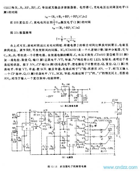
See as the above equations, the discharging time is longer that charging time,i.e the pulling time of relay J is longer than its releasing time, the fan generates gusts. And the intervals of the gusts can be changed by adjusting RP2. IC2(CD4022) is a octal counter/pulse distributor, which consists a counting circuit with C2,R5,R7 and so on. At the moment of power-on, the voltage on C2 doesn't mutate, and the reset terminal(R) (15-pin) of CD4022 is imposed with a high LEV, which lead to the high LEV of Q0 terminal(2-pin), and VT2 is conducting and the indicating LED2 of 0 gear glows green beams that means it is ready to run.
(View)
View full Circuit Diagram | Comments | Reading(462)
The 555 simple natural wind analog control circuit
Published:2011/5/29 22:10:00 Author:Borg | Keyword: natural wind, analog control
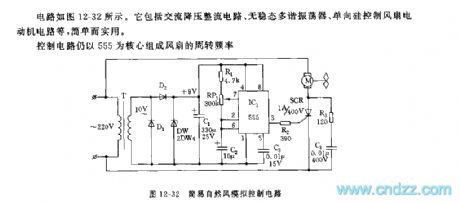
The circuit is as shown in Figure 12-32, which includes the AC step-down rectifier circuit, non-steady multi-resonate oscillator and the motor circuit of single-way silicon control fans, etc. It is simple and practical.
The control circuit is based on 555, and the rotating frequency of the fan is fc=1.44/(R1+PR1)C2, which is about 0.5~30Hz, by adjusting RP1, we can change the time parameters of charging and discharging, so the rotating speed of the fan can be changed, i.e the strength of the wind can be controlled. When the rotating speed is low, the wind is like a breeze. In the figure, R3,C4 and SCR connect in a parallel way, which is used to protect the controllable silicon SCR. (View)
View full Circuit Diagram | Comments | Reading(665)
The 555 discontinuous running timer circuit
Published:2011/5/30 3:34:00 Author:Borg | Keyword: discontinuous, timer circuit
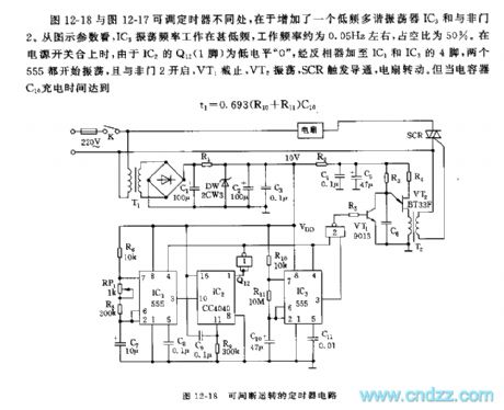
The the difference between adjustable timers in Figure 12-18 and Figure 12-17 is that the earlier is added with a low-frequency multi-resonate oscillator IC3 and a NAND. Judging from the parameters in the figure, the oscillation frequency of IC3 is very low, which is about 0.05Hz, and its duty cycle is 50%. When the power supply switch is closing, as Q12(1-pin) of IC2 is at a low LEV 0 , and the LEV is added to the 4-pin of IC1 and IC3 by the inverter, then both of the 555 start to oscillate, and the NAND 2 opens, VT1 is blocked, VT2 shakes, SCR is triggered and conducting, the fan runs.
(View)
View full Circuit Diagram | Comments | Reading(656)
The 555 natural wind circuit of long timing
Published:2011/5/29 22:33:00 Author:Borg | Keyword: natural wind, long timing
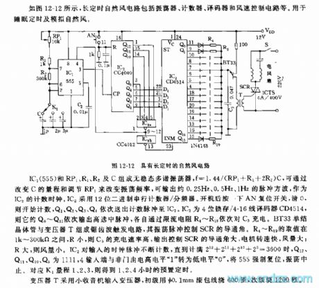
Figure 12-12 the natural wind circuit of long timingIC1(555),RP1,R1,R2 and C consist a non-steady multi-resonate oscillator whose f is 1.44/(RP1+R1+2R2)C, and the frequency can be changed by changing the measuring range of C and adjusting RP1, the frequencies of the output pulse square waves are 0.25Hz,0.5Hz and 1Hz, respectively, which can be the counting clock of IC2. The circuit computes with a 12-degree binary series counter/frequency distributor. When it is on, press the reset switch AN and clean the former numbers, then it starts to count, Q1,Q2,Q3 and Q4 deliver counting pulse to IC3 in turn. IC3 is a 4 bit lock/4-16 wire decoder CD4514. (View)
View full Circuit Diagram | Comments | Reading(503)
Identifying the same polarity of the coil
Published:2011/5/30 4:10:00 Author:Seven | Keyword: same polarity


76.identifying the same polarity of the coilIf we want to know the same polarity of the primary and second stage coil in a transmitter, we can judge by using identifiers which consists of elements like controllable silicons, etc. See as the circuit, it is designed according to the conducting condition of controllable silicons. At the moment of power-on, the primary coil L1 is generating sensing LEV of which the left is negative and the right is positive. If 1 and 3 are the same polarity, the pole of 3 will sense a positive LEV, put the two positive LEV on the positive pole and control stage,respectively, then the controllable silicon is conducting and the LED is glowing.
(View)
View full Circuit Diagram | Comments | Reading(697)
the Integral reset circuit of improved I
Published:2011/5/30 7:14:00 Author:Ariel Wang | Keyword: Integral, reset, improved I


From below we can see that the time constant of discharge circuit usually far less than of charge circuit.At this time,the unreliable phenomenon of power on reset caused by switch on and off can be controlled . As the time constant of discharge is too short,it reduces the insensitiveness of voltage fluctuation to power-supply when the reset circuit is at work.
(View)
View full Circuit Diagram | Comments | Reading(635)
the circuit of hardware in SD1077 singlechip system
Published:2011/5/29 23:15:00 Author:Ariel Wang | Keyword: hardware, singlechip system

The circuit of hardware in SD1077 singlechip system is as the chart below:
(View)
View full Circuit Diagram | Comments | Reading(427)
the reset circuit of MAX706P
Published:2011/5/29 23:15:00 Author:Ariel Wang | Keyword: reset

The reset circuit of MAX706P is as the chart below:
(View)
View full Circuit Diagram | Comments | Reading(407)
the circuit of static digital display
Published:2011/5/29 23:17:00 Author:Ariel Wang | Keyword: static , digital, display

It can be divided into static display and dynamic display as there are two ways of display.Here what we talked about is static display.It is two-bits static digital display.Its main function is displaying the serial number of LED light which is on.If L1 light is on,digital tube will display 11.If L2 is on,digital tube will display 22,ect.The design of the circuit is composed of two 8-bits shift register (74HC164), two 8-sections LEB digital tube( Common anode) and two 8×330Ω exclusion .
(View)
View full Circuit Diagram | Comments | Reading(449)
the joint circuit of ADS7805 and TMS320F206
Published:2011/5/29 23:18:00 Author:Ariel Wang | Keyword: joint

The 16-bit fixed point DSP TMS320F206 of T1 company is low power device.It adopts improved Harvard structure .It has one procedure base line,3 data base lines,assembly lines and so on.When TMS320F206 externally connects the 16MHZ crystal oscillator ,and the control mode of working clock is ×1,you can connect /CS pin to DSP's /RD signal pin.But in order to reduce the controlling line,you can reduce /CS's pin to low level .You can connect R/C's pin to /RD's signal pin and you can connct R/C's pin to DSP expanding output port.But /BUSY signal can only be connected to common input port.For example,DSP's IO port,expanding chip 74LS244's input port,ect.
(View)
View full Circuit Diagram | Comments | Reading(504)
the joint circuit of DSP and 8237
Published:2011/5/29 23:19:00 Author:Ariel Wang | Keyword: joint, DSP


The circuit as the chart below provides DMA service signal from 4 channels' peripheral demands.And 8237 has AEN pin.It can satisfy all requests of chart 1.So it reallizes the interface between DSP and the sound card.In actual work,we based on the situation of usage of the sound card in PC to set up whether 8237's DREQ1 or DACK1 can be the play passage,whether 8237's DREQ3 or DACK3 can be the collecting passage,whether the break application signal IRQ7 goes through GAL16V8 becoming reversed with DSP'spin or not.
(View)
View full Circuit Diagram | Comments | Reading(489)
The circuit based on optic radiation TAD6101
Published:2011/5/30 7:14:00 Author:Ariel Wang | Keyword: optic radiation
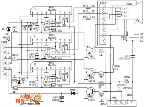
View full Circuit Diagram | Comments | Reading(780)
the power-supply circuit-fixed of adjustable and DC part 14
Published:2011/5/29 20:14:00 Author:Ariel Wang | Keyword: adjustable, DC, circuit-fixed
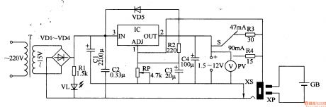
The working principle of circuit
This DC power-supply circuit-fixed is made up by the circuit of dropped-down and commutated voltage,steady output circuit and constant current output circuit.See chart 5-18 below.
After the 220V AC voltage is dropped down through T,commutatedthrough VDl-VD4.It is connected to the third foot (the edge of input) of IC directly,as the input voltage of regulator.It is connected to VL through Rl.And then it light VL up.
When the plug XPisnot plugged into the socket XS,the 15VAC voltage on the second winding of T is commutated through VDl-VD4,filtered through Cl and numberous regulation.Then it outputssteady DC voltage through the second foot of IC. You can adjust the resistence of RP,in order to make the output DC voltage contiously adjustable between 1.25-12V.
(View)
View full Circuit Diagram | Comments | Reading(538)
Power-supply of adjustable DC steady voltage part 11
Published:2011/5/29 20:15:00 Author:Ariel Wang | Keyword: adjustable, DC , steady voltage
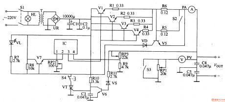
After SLis gotten through, HL is lighted up.The 220V AC voltage is dropped down through T,commutated through UR,filtered through C1 and C2 and regulated through voltage regulation output circuit.It generates 5-30V DC voltage.You can adjust the resistance of RP2(output voltage fine adjustment control ) and RP3(output voltage coarse adjustment ). It can change the conduction ability of Vl-V4 and the voltage of emitter (b,e pole) ,then it wil change the output voltage.When it's over loaded by some reasons,try to make the output electric current increase to a certain level.Try to conduct V5,to stop V7 ,to make the 3 feet output voltage of IC 0V and to stop Vl-V4.Then the output voltage is disappeared.
(View)
View full Circuit Diagram | Comments | Reading(2132)
Power-supply of adjustable DC steady voltage part 8
Published:2011/5/29 23:26:00 Author:Ariel Wang | Keyword: adjustable, DC , steady voltage

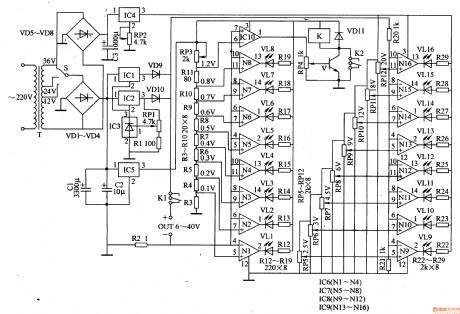
The 220V AC voltage is dropped down through T,commutated through VD1-VD4,filtered through C1 and C.And it is regalated by lCl-IC3,RPl,Rl,VDg and VDlO.Then it goes through the contactor K1 of electric relay K .It provides load(withelectrical equipment) .Or it may charge up storage battery. It is voltage-regulated to +6V through IC5, being as the working voltage for IC6,1C7,IClO and K . The AC voltage regulated through T should commutate through VD5-VD.It filtered through C3 and voltage-regulated through IC4 and RP2.It generates +20V voltage as the working power-supply for IC5 and IC9. In order not to make the voltage drop too much when the voltage goes through the input end to the output end .You can use voltage option switch S to choose the voltage of 12V,24V and 36V AC secondary side of T.Adjust the resistance of RP1.Then its output end (OUT) can generate DC voltage of 6-40V.
(View)
View full Circuit Diagram | Comments | Reading(672)
the AD9850 circuit
Published:2011/5/29 23:30:00 Author:Ariel Wang | Keyword: circuit

The AD9850 circuit is as the chart below:
(View)
View full Circuit Diagram | Comments | Reading(492)
the independent oscillator divider circuit of watchdog delicated chip TPS3823
Published:2011/5/30 10:29:00 Author:Ariel Wang | Keyword: independent, oscillator divider , watchdog, delicated chip

①Because the clock of the watchdog is dependent,the counting clock and the system belong to the same frequency division link.The watchdog won't operate effectively when the system have some problems.②The clock can use software to set up.When the setting up is failed,the clock may fail as well. Without clock,watchdog can't work well.③Some watchdog need software to set up and start.So when the start fails and initialization unactivated,CPU might jump to random code.It may stop the watchdog.Theoretically,the design has the unreasonable part.Based on the analysis above,we adopt off chip watchdog using dedicated chip TPS3823.The experimental circuit is seen as below:
(View)
View full Circuit Diagram | Comments | Reading(663)
INA166 Input Stable Network Circuit
Published:2011/5/21 21:50:00 Author:Robert | Keyword: Input, Stable, Network

The INA166 Input Stable Network Circuit is shown in the picture below. A very low signal source's resistance (lower than 10Ω) can cause the INA166 to have self-oscillation. By adding two small inductance and small resistance at its input port it can make up a neywork which can minimize the self-oscillation trend. Althrough in INA166's other typical applications there is no inductance and resistance network, it can be added the inductance and resistance network to limit the self-oscillation when it is needed.
(View)
View full Circuit Diagram | Comments | Reading(529)
Rectifier Circuit
Published:2011/5/21 1:11:00 Author:Robert | Keyword: Rectifier

This circuit can change the input AC signals to DC signals. If the input signal has a low frequency, the capacitance C1 in input port can be cancelled.
In the negative half cycle, the operational amplifier IS1's output signals are connected through diode D1 (withcut-off voltage 0.7V) and would be isolated from the adding point through the diode D2. The operational amplifier IS2 isworking as out-phase voltage follower device.
In the positive half cycle, the IS1 isworking as out-phase amplifier and is connected to the adding point through R2. In input port, theresistance R3 and the resistanceR2 are made up a negative feedback loop circuit.
(View)
View full Circuit Diagram | Comments | Reading(478)
Eye-care Lamps (the 5th)
Published:2011/5/20 1:55:00 Author:Felicity | Keyword: Eye-care Lamps (the 5th)
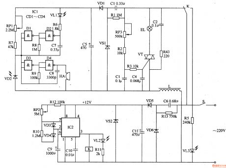
Work of the circuit
The circuit consists of power circuit, timing control circuit, LED indicating circuit, light changing circuit, light examine circuit and acousto-optic alarm circuit (It is showed in picture 9-72.).
Turn on the switch S and timing control circuit is supplied with +12V working voltage. And the voltage separates into two parts. One lightens the EL in the meantime the other one supplies 9V voltage to light examine circuit and acousto-optic alarm circuit.
Change the value of RP1 to change the sensitivity of light examining circuit. And change the value of RP2 to change the regular timer. (View)
View full Circuit Diagram | Comments | Reading(391)
| Pages:1831/2234 At 2018211822182318241825182618271828182918301831183218331834183518361837183818391840Under 20 |
Circuit Categories
power supply circuit
Amplifier Circuit
Basic Circuit
LED and Light Circuit
Sensor Circuit
Signal Processing
Electrical Equipment Circuit
Control Circuit
Remote Control Circuit
A/D-D/A Converter Circuit
Audio Circuit
Measuring and Test Circuit
Communication Circuit
Computer-Related Circuit
555 Circuit
Automotive Circuit
Repairing Circuit