Circuit Diagram
Index 1820
monolithic temperature sensor circuit
Published:2011/5/29 8:13:00 Author:chopper | Keyword: monolithic, temperature sensor
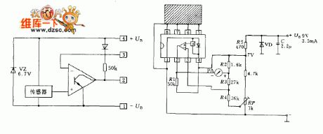
Integrated circuit LM3911 is a silicon sensor composed of operational amplifier and voltage regulator circuit.It can be a simple electrical thermometer only by using a few external components.Transistor is used as a temperature-sensing element on the silicon chip.The voltage of base and emitter of the transistor varies with temperature changes.When the temperature rises,the voltage will increase.Outside temperature intussuscepted from a copper billet will be passed on to the temperature sensor.The copper billet will be connected to pins 5~8 of the integrated circuit and the inside parts of these pins are connected to temperature sensor.
(View)
View full Circuit Diagram | Comments | Reading(599)
Scintillation Caution Light (1)
Published:2011/5/27 6:17:00 Author:Sue | Keyword: Scintillation, Caution Light

When the circuit begins to work, V1 will output oscillator current. When the current goes through the LED, the LED will be illuminated from time to time. HL is twinkling.
When it is in the daytime, RG has a low resistance value, and the voltage is low too. V2 is disconnected and the circuit doesn't work. HL is not illuminated. When it is in the dark, RG's resistance value becomes larger and the voltage becomes higher. Multivibrator consists of V1 V2 begins to work. The red scintillation caution light HL will begin to twinkle. (View)
View full Circuit Diagram | Comments | Reading(494)
Negative feedback circuit of Pure dc current made by LM3886
Published:2011/6/2 5:49:00 Author:chopper | Keyword: Negative feedback circuit, Pure dc current

LM3886 is of excellent performance and win its popularity on sound system in recent years.Many power amplifiers use it as the latter stage amplifier or supper bass amplifying circuit directly. It uses LM3886TF as power amplifier which is a new hi-fi stereo amplifier integrated circuit produced by US company NS(a semiconductor company of State) and uses operational amplifier NE5532 or AD827 as leading linear amplifier and tone amplifier.
(View)
View full Circuit Diagram | Comments | Reading(3247)
structure circuit of single-channel signal processing
Published:2011/6/1 2:28:00 Author:chopper | Keyword: structure circuit, single-channel signal processing
View full Circuit Diagram | Comments | Reading(466)
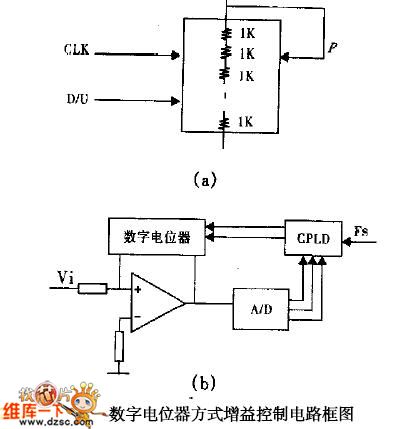
Gain Control Circuit with Digital Potentiometers
Published:2011/6/1 2:11:00 Author:chopper | Keyword: Gain Control, Digital Potentiometers
View full Circuit Diagram | Comments | Reading(440)
Fast integrator with low input current circuit
Published:2011/6/1 2:08:00 Author:chopper | Keyword: Fast integrator, low input current
View full Circuit Diagram | Comments | Reading(848)
EW-8W electronic ballast circuit
Published:2011/5/31 8:01:00 Author:chopper | Keyword: electronic ballast
View full Circuit Diagram | Comments | Reading(1657)
digital isolation circuit
Published:2011/5/30 5:08:00 Author:chopper | Keyword: digital isolation

This circuit uses photocoupler to reach a absolute isolation between two digital circuit.The input signal even if it is low to 4V can also change the state of output,and the circuit will not be punctured even though a input peak around +100V.Q1,Q2 form current stabilizer and limit the loop current of the input end through the optoelectronic isolator in 7mA. Zener diode CR2 offers reference voltage and controls the current through R2.Schmitt trigger on the output end eliminates oscillation. (View)
View full Circuit Diagram | Comments | Reading(657)
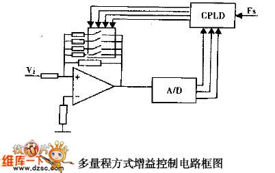
multrirange gain control circuit
Published:2011/5/29 22:12:00 Author:chopper | Keyword: multrirange, gain control
View full Circuit Diagram | Comments | Reading(398)
The fixed cycle pulse generator circuit with the adjustable duty ratio
Published:2011/5/25 6:15:00 Author:Christina | Keyword: fixed cycle, pulse generator, adjustable, duty ratio
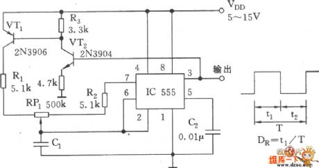
As the figure shows, the astable multivibrator is composed of the 555, VT1, VT2, R1, R2, RP1 and C1. In this figure, the capacitor C1 has the independent charging and discharging circuit, when you adjust RP1, you can change the charging and discharging time constants, but can not change the oscillation frequency. Before C1 is charged to the 2/3VDD threshold electrical level, pin-3 has the high electrical level, that means during the time of t1, VT2 conducts, VT1 fully conducts, so VT1 has the small impedance. By adjusting RP1, you can change the duty ratio between 2% to 98%, the period can not be changed.
(View)
View full Circuit Diagram | Comments | Reading(895)
Radio launch alarm crystal oscillation frequency stabilizing FM circuit
Published:2011/5/25 18:54:00 Author:Christina | Keyword: Radio launch, alarm, crystal oscillation, frequency stabilizing, FM circuit
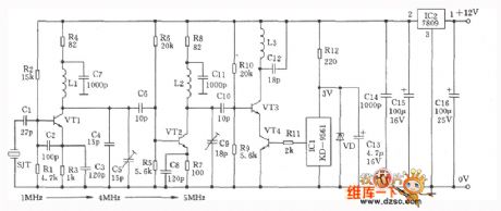
The crystal oscillation frequency stabilizing FM circuit is as the figure shown, this circuit can be used in the radio launch alarm. So it has the features of simple to use, stable performance, small size, low cost, it is one kind of high cost-effective circuit.
Performance indexes:
Operating frequency: 85 to 120MHz;
output power: 5~200mW(adjustable);
Launch distance: 50~1000m;
operating voltage: 9VDC;
operating current: 50 to 60 mA.
The transistors VTl and VT2 use the 3DGl30C、β≥50, the VT3 uses the L413K amplifier tube, the VT4 is 8050、β≥80. The voltage stabilization diode VD uses the 3V, 0.5W voltage stabilization tube. ICl is the KD-9561 simulation soft package sound integrated circuit. All the high-frequency circuit oscillation capacitances uses the high frequency ceramic or the polyester capacitor.
(View)
View full Circuit Diagram | Comments | Reading(499)
Digital control type astable multivibrator circuit
Published:2011/5/25 20:16:00 Author:Christina | Keyword: Digital control, astable multivibrator

As the figure shows, the oscillator is composed of the DAC, the mirror current source and the 555 oscillator. The oscillation frequency is related to the input data size and the control reference voltage. IC1 uses the D/A conversion circuit DAC0800 LCN, this circuit is the 8-bit DAC, it changes the data into the analog signal and adds the signal to the mirror current source VT1's b port, so it controls the VT2's integrated electrode current - 555 oscillator C's charging current, and also changes the frequency of the oscillator. (View)
View full Circuit Diagram | Comments | Reading(1510)
MC3357 small power FM intermediate frequency integrated circuit typical application circuit
Published:2011/5/25 20:28:00 Author:Christina | Keyword: small power, FM, intermediate frequency, integrated circuit, typical application

The MC3357 is designed as one kind of small power FM intermediate frequency integrated circuit that is produced by the MOTOROLA company, and it can be used in the FM duplex communication equipment's FM intermediate frequency circuit, the frequency mixer circuit, the noise suppression and lagging circuit, the active filter amplification circuit, the amplitude limit amplification circuit, the modem circuit and other subsidiary function circuits. The internal circuit block diagram and the typical application circuit which is composed of the MC3357 IC are as shown in the figure.
(View)
View full Circuit Diagram | Comments | Reading(2934)
DS8922 differential line driver and receiver circuit
Published:2011/5/25 21:27:00 Author:Christina | Keyword: differential line, driver, receiver


The DS8922 meets the requirement of EIA standard RS-422, the output delay time is 0.5ns; the propagation delay time ≤12ns; it uses the high differential or common-mode input mode; the voltage range is ±7V; the voltage is output by the complementary driver; it can be used to non-polarity differentially drive the twisted-pair lines or the parallel transmission lines; the complementary output is the logic. The DS8922 can be used in the occasions which are meet the ST506, ST412 and ESDI wheel drive standards, and it is compatible with the CMOS circuit.
The internal circuit block diagram of the DS8922:
The typical application circuit:
(View)
View full Circuit Diagram | Comments | Reading(1012)
Differential mode signal and differential mode voltage amplification factor Aud circuit
Published:2011/5/26 1:00:00 Author:Christina | Keyword: Differential, mode signal, mode voltage, amplification factor, Aud

Differential mode signal--Add the same amplitude opposite polarity signals on the differential amplification tube T1 and T2's base electrode. As the figure shows:
The function of the differential mode signal: because the signals' polarities are opposite, so T1's collector electrode voltage reduces, T2's collector electrode voltage increases, and the variable quantitiy absolute values of T1 and T2 are the same, so Uod=Uc1=Uc2=2Uc1 (or 2Uc2) (View)
View full Circuit Diagram | Comments | Reading(389)
PCA8581 I2C port 128×8-bit E2PROM circuit
Published:2011/5/26 1:24:00 Author:Christina | Keyword: I2C port, 128×8-bit, E2PROM


The PCA8581 has the 128×8-bit E2PROM address; the data can be transmitted by two bidirectional buses (the I2C) through the serial port; it has three address pins A0, A1, A2, the function is to ensure the hardware address; also it can directly drive eight devices to the bus but needs no additional accessories, it can be used in the applications which are related to the industrial computer storage control projects.
Internal circuit blockdiagram:
Typical application circuit:
(View)
View full Circuit Diagram | Comments | Reading(520)
Common-mode signal and common-mode voltage magnifacation Auc circuit
Published:2011/5/26 1:55:00 Author:Christina | Keyword: Common-mode signal, common-mode voltage, magnifacation , Auc

The Common-mode signal--Adds the same amplitude opposite polarity signals on the differential amplification tube T1 and T2's base electrode. As the figure shows:
The function of the common-mode signal: it has the synclastic effects to the two tubes, it will cause the commensuration increase of the current and the commensuration reducing of the collector potential, so the two tube's collector electrode output common-mode voltage Uoc is zero. (View)
View full Circuit Diagram | Comments | Reading(439)
Soil humidity tester circuit
Published:2011/5/30 1:27:00 Author:Christina | Keyword: Soil, humidity, tester

The circuit principle: this soil humidity tester circuit is composed of the humidity detection probe, the transistor V, the diodes VDl-VD4, the LEDs VLl-VL5, the potentiometer RP, the power switch S and the battery GB. When the humidity detection probe is not in the soil or the soil is too dry, the V and the VDl-VD4 are in the cut-off state, VL1~VL5 do not emit light. When the soil has certain humidity, the soil moisture makes the resistance between the two electrodes of the humidity detection probe lower and lower, V conducts, VLl-VL5 turn on one by one. The greater the soil moisture is, the stronger the V conduction capacity is, the more number of LEDs will turn on.
(View)
View full Circuit Diagram | Comments | Reading(1216)
Thermocouple temperature measurement circuit with the cold contact point compensation
Published:2011/5/26 8:22:00 Author:Christina | Keyword: Thermocouple, temperature measurement, cold contact point, compensation
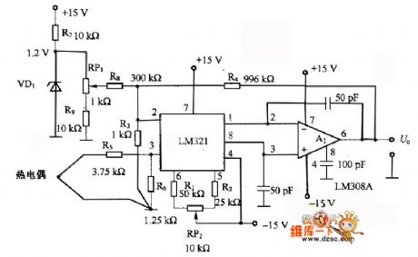
The thermocouple temperature measurement circuit with the cold contact point compensation is as shown. This circuit is composed of the preamplifier LM321 and the operational amplifier LM308A. The LM321 has the temperature characteristic of lμV/℃. If the maladjustment voltage is zero, the temperature drift is zero too; if there is the maladjustment voltage, it will produce the temperature drift, this temperature drift can be used in the thermocouple's cold contact point compensation.
(View)
View full Circuit Diagram | Comments | Reading(2535)
Water level indicator circuit (4)
Published:2011/5/29 22:55:00 Author:Christina | Keyword: Water level, indicator
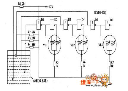
The operating principle: this circuit is composed of the water level detection circuit and the LED driving circuit, as the figure shows.
The water level detection circuit is composed of the water level detection electrodes a-d, the resistors Rl-R4, the Dl, D3, D5 of the NAND gate ICs Dl-D6.
The D driving circuit is composed of the IC, the discoloration LEDs LEDl-LED3 and the resistors R5-R7.
When the water level detection electrode d is in the water, the electrode connects with the electrode d through the resistance of water, the NAND gate Dl's input port has the high electrical level, and it's output port has the low electrical level, D2's output port has the high electrical level. When the water level is lower than the electrode d, Dl's input port has the low electrical level and the output port has the high electrical level, D2's output port has the low electrical level to make the VL1 to send out the red light. (View)
View full Circuit Diagram | Comments | Reading(1387)
| Pages:1820/2234 At 2018011802180318041805180618071808180918101811181218131814181518161817181818191820Under 20 |
Circuit Categories
power supply circuit
Amplifier Circuit
Basic Circuit
LED and Light Circuit
Sensor Circuit
Signal Processing
Electrical Equipment Circuit
Control Circuit
Remote Control Circuit
A/D-D/A Converter Circuit
Audio Circuit
Measuring and Test Circuit
Communication Circuit
Computer-Related Circuit
555 Circuit
Automotive Circuit
Repairing Circuit

