
Circuit Diagram
Index 1810
Electronic pressure switch circuit diagram
Published:2011/5/29 2:35:00 Author:Lucas | Keyword: Electronic pressure switch
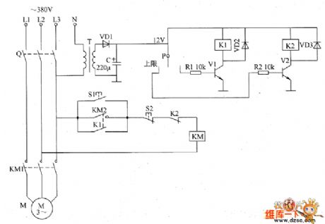
The electronic pressure switch circuit consists of the power circuit and pressure detection control circuit, the circuit is shown as the chart. Power circuit is composed of the power transformer T, rectifier diode VD1 and filter capacitor C. Pressure detection control circuit consists of the electric contact pressure gauge P, resistors R1 and R2, transistors V1 and V2, the relays K1 and K2, and diodes VD2, VD3. M is the air compressor motor, KM is the exchange of contact, Q is the knife switch, S1 is the start button, S2 is the stop button. The AC voltage between phase line L3 and zero line bucked by T, rectified by VD1 and filtered by C can provide 12V DC voltage for K1 and K2. R1 and R2 use 1/4W metal film resistors, or carbon film resistors. C uses aluminium electrolytic capacitor with voltage in 16V. VD1 ~ VD3 use 1N4007 silicon rectifier diodes. V1 and V2 use S8050, C8050 or 3DG8050 silicon NPN transistors.
(View)
View full Circuit Diagram | Comments | Reading(3409)
High voltage static generator circuit diagram 1
Published:2011/6/8 4:38:00 Author:Lucas | Keyword: High voltage , static generator

The high voltage static generator circuit is composed of the power switch S, power transformer T, rectifier diodes VD1 ~ VD9, capacitors C1 ~ C9, resistors R1 ~ R4, voltmeter PV and ammeter PA, and the circuit is shown as the chart. R1 ~ R4 select 1W high-voltage resistors. C1 ~ C9 select high voltage ceramic capacitors with the voltage in 30kV. VD1 ~ VD9 select silicon rectifier stack with the voltage in 30kV (it also can replaced by two silicon rectifier stacks connected in series with the voltage in 18 ~ 20KV)such as the model of 2CGL30, 2DGL30. PV chooses 0 ~ 100kV high-voltage voltmeter. PA selects 0 ~ 100A current meter. S uses 220V bipolar switch with the contact current capacity being greater than 5A.
(View)
View full Circuit Diagram | Comments | Reading(2396)
Metal detector circuit diagram 8
Published:2011/6/7 20:00:00 Author:Lucas | Keyword: Metal detector

The metal detector circuit is composed of the probe oscillator, PLL phase-locked loop circuit and the audio alarm circuit, and the circuit is shown as the chart. Probe oscillator is composed of the detection coil L, transistor VI, resistors RI ~ R3, capacitors C1 ~ C5. PLL phase-locked loop circuit consists of integrated circuit IC1, resistors R4 ~ R8, capacitors C7 ~ Cll. Audio alarm circuit is composed of the transistor V2, comparision amplifier integrated circuit IC2, buzzer HA, resistors R9 ~ R14. R1 ~ R14 use 1/4W carbon film resistors or metal film resistors; R15 uses 1/2W metal film resistor. RP uses small potentiometer or variable resistor. V1 and V2 use 59018 or 2SC1815 NPN silicon transistors.
(View)
View full Circuit Diagram | Comments | Reading(6464)
Metal detector circuit diagram 7
Published:2011/6/7 19:55:00 Author:Lucas | Keyword: Metal detector
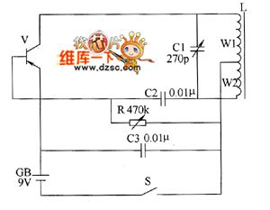
The metal detector uses LC single-tube oscillator circuit, and the circuit is shown as the chart. In the circuit, V is oscillating tube, L is the detection coil, C1 is the resonant capacitor. The LC single-tube oscillator circuit works after turning on the power switch S, the speaker of semiconductor superheterodyne radio will issue sounds with the frequency around 1kHz. When the detection coil L detects underground metal, the sound frequency of the speaker becomes high. R selects variable resistor. C1 uses variable capacitor (270P single sealed); C2 and C3 use high-frequency ceramic or glass glaze capacitors. V selects 3AG1 or 3AGll high frequency low power PNP germanium transistor. CB uses 9V tandem battery. Adjusting the resistance of R can make the operating current of machine be about 15mA.
(View)
View full Circuit Diagram | Comments | Reading(1049)
Metal detector circuit diagram 6
Published:2011/6/7 19:45:00 Author:Lucas | Keyword: Metal detector

The metal detector circuit is composed of the probe oscillator, reference oscillator, oscillation signal processor, mixing amplifier and ammeter PA and other components, and the circuit is shown as the chart. Probe oscillator is composed of the oscillating tube VI, explore coil L1, capacitors C1 ~ C4 and resistors R1 ~ R3 and so on. Reference oscillator is composed of the oscillating tube V2, inductor L2, capacitors C6 ~ C9 and resistors R2 ~ R4 and so on. Oscillation signal processor consists of six NOT gate (Dl ~ D6) integrated circuit IC and the external RC components. Hybrid amplifier is composed of the diode YD, resistors R12, R13, capacitors C13 and field-effect transistor VF. V1 and V2 use 59018 silicon NPN transistor. VF selects V20A field effect transistor.
(View)
View full Circuit Diagram | Comments | Reading(4867)
Metal detector circuit diagram 5
Published:2011/6/8 4:00:00 Author:Lucas | Keyword: Metal detector

The metal detector circuit consists of oscillator and sound-light alarm circuit, and the circuit is shown as the chart. Oscillator circuit consists of inductor L, capacitor C1, sensor switch integrated circuit IC1 (includes oscillator, detector and comparator circuit, etc.) and the peripheral components. Sound-light alarm circuit consists of four NOR gate integrated circuit IC2 (Dl ~ D4) and the light-emitting diode VL, speaker BL and other components. R1 ~ R6 select 1/4W carbon film resistors. C1 ~ C4 select ceramic capacitors. VL selects Φ5mm high-brightness light-emitting diode. V uses S9013 or C8050 silicon NPN transistor. IC1 uses TDA0161D sensor switch integrated circuit; IC2 selects CD4001 four NOR gate integrated circuit.
(View)
View full Circuit Diagram | Comments | Reading(2964)
Metal detector circuit diagram 4
Published:2011/6/7 19:39:00 Author:Lucas | Keyword: Metal detector
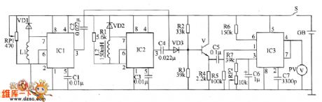
The metal detector circuit is composed of the probe oscillator, reference oscillator, mixer and signal display and other components, and the circuit is shown as the chart. Probe oscillator consists of time-based integrated circuit IC1, inductor L1, potentiometer RPI, diode VD1 and capacitors C1, C2. Reference oscillator (reference oscillator) circuit is composed of the time-base integrated circuit IC2, inductor L2, diode VD2, resistor RI and capacitors C3, C4. Mixer is composed of the transistor V, diode VD3 and resistors R2 ~ R4. Signal display circuit consists of integrated circuit IC3, voltage meter PV and peripheral capacitance resistance element. R1 ~ R7 choose 1/4W or 1/8W carbon film resistors. V uses 3DG6 or S9018 silicon NPN transistor.
(View)
View full Circuit Diagram | Comments | Reading(1341)
Metal detector circuit diagram 3
Published:2011/6/7 19:34:00 Author:Lucas | Keyword: metal detector

The metal detector is composed of the probe oscillator, reference oscillator and audio amplifier and other components, and the circuit is shown as the chart. Probe oscillator consists of transistors VI, V2 and detection coil L1, capacitor C1 and so on. Reference oscillator consists of transistors VI, Y3 and inductor L2, capacitor C3 and other components. Audio amplifier is composed of audio power amplifier IC IC, volume potentiometer RP and capacitors C6 ~ C8 RP and so on. R1 uses small or variable resistor; R2 ~ R5 select 1/4W metal film resistors. RP uses small membrane potentiometer. C1 uses high-frequency ceramic capacitor; C2, C5 ~ C8, CIO use aluminum electrolytic capacitor with the voltage in 10Y; C3 uses ceramic fine capacitor; C4, C9 select polyester or monolithic capacitors.
(View)
View full Circuit Diagram | Comments | Reading(4807)
Metal detector circuit diagram 2
Published:2011/6/8 4:09:00 Author:Lucas | Keyword: Metal detector

The metal detector circuit is composed of the power circuit, sine wave oscillator, PLL phase-locked loop circuit and hybrid amplifying circuit, and the circuit is shown as the chart. Power circuit is composed of the batteries GBI, GB2, filter capacitors C1, C2, and the power switch s (Sa, Sb). Sine oscillator circuit consists of transistor VI, detecting coil L, capacitors C3 ~ C5 and resistors RI, R2. PLL phase-locked loop circuit IC consists of dual time-base integrated circuit and resistos R3, potentiometer RP1, capacitors C6 ~ C8. Hybrid amplifying circuit is composed of the transistors V2, V3, resistors R4 ~ R6, potentiometer RP2 and ammeter PA. R1 ~ R6 use l/4W or l/8W carbon film resistors.
(View)
View full Circuit Diagram | Comments | Reading(4151)
Electronic rodent repeller circuit diagram 4
Published:2011/6/7 4:39:00 Author:Lucas | Keyword: Electronic rodent repeller

The electronic rodent rodent repeller circuit is composed of the time oscillator, mew generator, audio power amplifier and flash control circuit, and the circuit is shown as the chart. Oscillator circuit is composed of the time base timer integrated circuit IC1, resistor R1, potentiometers RP1, RP2, diodes VD1 ~ YD3, capacitors C1, C2, and relay K1. Mew generator is composed of the sound generator circuit IC IC2, resistor R2, potentiometer RP3 and capacitors C3 ~ C5. Audio power amplifier is composed of the power amplifier integrated circuit IC3, capacitors L6 ~ C8 and speaker BL. Flash control circuit consists of transistor V, resistor R3, relay K2, diode HL and small bulb VD4.
(View)
View full Circuit Diagram | Comments | Reading(1013)
Electronic rodent repeller circuit diagram 2
Published:2011/6/7 4:39:00 Author:Lucas | Keyword: Electronic rodent repeller

The electronic rodent repeller circuit is composed of the timer circuit, mew generator and power amplifier and other components, and the circuit is shown as the chart. Timer circuit is composed of a time-base integrated circuit IC1 and the non-steady-state multivibrator composed of the related external components. Mew generator consists of integrated circuit IC2 and transistors V and so on. Power amplifier consists of integrated circuit IC3, and related peripherals RC components. R1 ~ R5 use 1/4W or 1/8W carbon film resistors. RP1 and RP2 can choose small solid-type potentiometer or variable resistor WH7. C1, C3 ~ C7 select aluminium electrolytic capacitor with the voltage in 16V; C2 and C8 select ceramic capacitors. VD1 and VD2 use 1N4148 silicon switching diodes. V uses 590I3 or 3DG12 silicon NPN transistor.
(View)
View full Circuit Diagram | Comments | Reading(1161)
Remote control toy car transmitter circuit
Published:2011/6/4 9:59:00 Author:John | Keyword: Remote control toy car

Remote control toy car transmitter circuit is shown below.
Potentiometer RV1 controls left and right wheels. Potentiometer RV2 controlsfront andrear wheels. Potentiometer RV3 makes slight adjustment forleft and right wheels. Potentiometer RV4makes slight adjustment for front andrear wheels. (View)
View full Circuit Diagram | Comments | Reading(4636)
VCO circuit
Published:2011/6/4 10:17:00 Author:John | Keyword: VCO
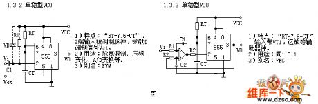
There are many monostable type VCO, which are all rather complex. For simplicity, we just divide it into 2 different units. The circuit without any auxiliary devices is 1.3.1. The circuit using transistors, operational amplifier and other auxiliary devices is 1.3.2. 2 common used circuits are shown in the figure.
1) Features: RT-7.6-CT , the end 2 is input with modulated pulse and the end 5 is set by modulated signal Vct 5.
2) Functions: modulation of pulse width, change of voltage-frequency, A / D change
3) Alias: PWM
(View)
View full Circuit Diagram | Comments | Reading(617)
Pulse start single stable circuit
Published:2011/6/4 10:47:00 Author:John
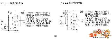
Pulse start single stable circuit can be divided into two different units. Two different units both are RT-7.6-CT and are input from end 2. 1.2.1. End 2 in the circuit has no components and is the simplest form. 1.2.2 Circuit has a differential circuit with RC.
1)Features: “RT-7.6-CT”, external pulse start or manual start.2)Formula: Td=1.1 RT*CT3)Functions: timing, time delay, flutter elimination, frequency division, frequency multiplication, strobe output and inspection for L、C rate
1)Features: “RT-7.6-CT”, external pulse start inputs to differential circuit with RC.2)Formula: Td=1.1 RT*CT3)Functions: timing, time delay, flutter elimination, frequency division, frequency multiplication, strobe output and inspection for L、C rate
(View)
View full Circuit Diagram | Comments | Reading(443)
Manual starting monostable circuit
Published:2011/6/4 10:58:00 Author:John
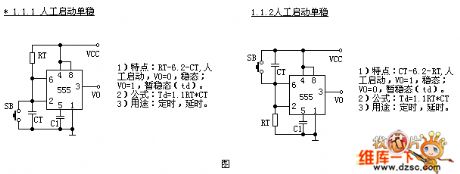
Manual starting monostable circuit is divided into two different units according to locations of timing resistor and timing capacitor. These two units are coded by 1.1.1 and 1.1.2 respectively. In the form of their input ends, that is to say that the structural characteristics of the circuit are: RT-6.2-CT and CT-6.2-RT .
1)Features: “RT-6.2-CT”, manual start,V0=0,steady-state;V0=1, temporary steady-state(td).2)Formula: Td=1.1 RT*CT3)Functions: timing and time delay.
1)Features: “CT-6.2-RT”, manual start,V0=0,steady-state;V0=1, temporary steady-state(td).2)Formula: Td=1.1 RT*CT3)Functions: timing and time delay.
(View)
View full Circuit Diagram | Comments | Reading(441)
Ring counter sequence pulse generator circuit
Published:2011/6/4 11:04:00 Author:John | Keyword: ring counter, sequence pulse generator
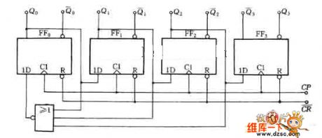
Ring counter sequence pulse generator circuit, just as shown in the figure, is a 4-output sequence pulse generator composed by a four-bit ring counter.
(View)
View full Circuit Diagram | Comments | Reading(1168)
Field-effect transistor US5U29、US5U30 internal circuit
Published:2011/6/4 11:20:00 Author:John | Keyword: Field-effect transistor
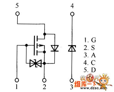
Field-effect transistor US5U29、US5U30 internal circuit is shown below.
(View)
View full Circuit Diagram | Comments | Reading(688)
power supply cavity monitoring circuit
Published:2011/6/4 11:29:00 Author:John | Keyword: power supply, cavity

Low level electricity logic circuit partially goes through the optical coupling, so that the power supply is isolated. When the power supply fails, the output level electricity is down to the logic level. Adjust the output of trigger to turn off the circuit.
The response time of the circuit is 2m8. When AC voltage is normally over zero, there is no effect on the circuit. Power consumption of the circuit is 50mW.
(View)
View full Circuit Diagram | Comments | Reading(838)
Field-effect transistor STG3P2M10N60B internal circuit
Published:2011/6/4 13:07:00 Author:John | Keyword: Field-effect transistor
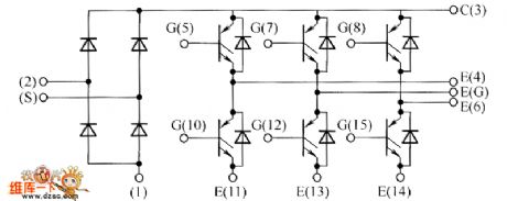
Field-effect transistor STG3P2M10N60B internal circuit is just shown below.
(View)
View full Circuit Diagram | Comments | Reading(648)
Field-effect transistor STE30NK90Z、STE40NK90ZD internal circuit
Published:2011/6/4 13:09:00 Author:John | Keyword: Field-effect transistor
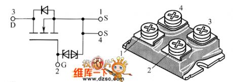
Field-effect transistor STE30NK90Z、STE40NK90ZD internal circuit is shown below.
(View)
View full Circuit Diagram | Comments | Reading(747)
| Pages:1810/2234 At 2018011802180318041805180618071808180918101811181218131814181518161817181818191820Under 20 |
Circuit Categories
power supply circuit
Amplifier Circuit
Basic Circuit
LED and Light Circuit
Sensor Circuit
Signal Processing
Electrical Equipment Circuit
Control Circuit
Remote Control Circuit
A/D-D/A Converter Circuit
Audio Circuit
Measuring and Test Circuit
Communication Circuit
Computer-Related Circuit
555 Circuit
Automotive Circuit
Repairing Circuit