
Circuit Diagram
Index 1671
The automatic for help alarm circuit
Published:2011/6/27 21:07:00 Author:Borg | Keyword: for help, alarm, automatic
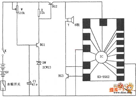
In the figure is the automatic for help alarm circuit. The circuit composes of the music integrated circuit IC(KD-9562), regulated pipe DW(2CW13), mercury switch, transistor, sliding rheostat W and the power supply, etc. It can be packaged in a plastic box and then put in the pocket, or fixed in the cane. When the person is erected, the mercury switch is off, the power supply is cut off, the circuit is not working and the music integrated circuit IC is silent. When the person is banding down (the alarm in the pocket) or the cane is falling on the ground, the mercury switch is closed.
(View)
View full Circuit Diagram | Comments | Reading(506)
The microwave burglarproof alarm circuit
Published:2011/6/27 21:24:00 Author:Borg | Keyword: microwave, burglarproof alarm

In the figure is the microwave burglarproof alarm circuit. This circuit consists of the simulated sound integrated circuit IC(CW9561), the LDR (MG45), the transistor and the power supply, etc. The alarm is installed in the closable room where there's some light, if the room is closed, the LDR will be in a high resistance because of no light, which makes the transistor BG2 blocked, so the simulated sound integrated circuit CW9561 is power-off, IC is not working, accordingly, the loudspeaker is silent. If the room is open, the LDR is in a low resistance due to the light.
(View)
View full Circuit Diagram | Comments | Reading(468)
The circuit of the microwave burglarproof alarm
Published:2011/6/27 21:35:00 Author:Borg | Keyword: microwave, burglarproof alarm
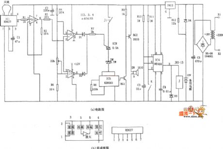
In the figure is the circuit of the microwave burglarproof alarm. This circuit consists of the Doppler FS sensor circuit IC1, the voltage comparator, the trigger single steady and delay circuit, stereo integrated circuit IC5 and so on. When the moving target is coming up, due to the FS between the reflected magnetic wave and the emitting wave, the Doppler FS sensor IC1 will output the DC LEV which is in positive proportion to the Doppler frequency generated when the object is moving, therefore, the detection and alert are done. And the microwave protection area is about 100m. The Doppler FS sensor IC1 is adopted with RD727 module.
(View)
View full Circuit Diagram | Comments | Reading(495)
The ultrasonic wave burglarproof circuit
Published:2011/6/27 21:47:00 Author:Borg | Keyword: ultrasonic wave, burglarproof
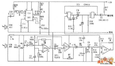
In the figure is the ultrasonic wave burglarproof circuit. The alarm contains the ultrasonic wave emitter and receiver and the decoder. In the circuit, the core of the ultrasonic wave emitter is the multi-resonance oscillator which consists of the 555, R19, R20, R21, W2, C12 and so on, and its oscillating frequency is f=1.44/(R21+Rw2十2R20+R19)C12, the frequency corresponding to the figured parameter is 40kHz+500Hz. After being reversed twice, the alternating square wave output by the oscillator is pushing the ultrasonic sensor UCM40T to output the ultrasonic pulse wave of 40KHz. When the wave encounters the moving object, the Doppler FS is generated.
(View)
View full Circuit Diagram | Comments | Reading(567)
The 555 pulse electric therapeutic apparatus circuit
Published:2011/6/27 22:11:00 Author:Borg | Keyword: pulse, electric therapeutic apparatus
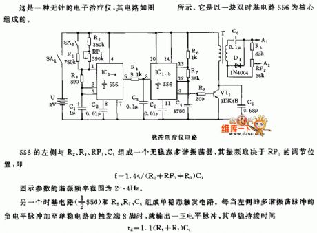
This is the stingless electric therapeutic apparatus, whose circuit is shown in the figure. It is formed based on a dual time-based circuit 556.
The pulse electric therapeutic apparatus circuit The left side of 555 composes an astable multi-resonance oscillator with R2, R3, RP1 and C1, whose oscillating frequency is decided by the position of RP1, i.e:F=1.44/(R2+RP1+R3)C1 The resonance frequency of the figured parameter is 2~4Hz. Another time-base circuit (1/2 556) composes a single stable trigger circuit. Once the passive LEV pulse of the resonance oscillating pulses on the left side is added on the 8-pin of the trigger terminal of the single steady circuit, a positive LEV pulse is output.
(View)
View full Circuit Diagram | Comments | Reading(521)
The touch burglarproof alarm circuit
Published:2011/6/27 20:19:00 Author:Borg | Keyword: burglarproof alarm

In the figure is the touch burglarproof alarm circuit. This circuit consists of the single steady trigger, the sound simulating circuit, the audio power supply amplifier circuit, the touching metal chip M, the rectifier filter circuit and so on. In the circuit, the time-based circuit 555, R1, R2 and C4 compose the single steady trigger, whose input signal, i.e the triggering signal past C3 when the touching metal chip M is touched, it is input from 2-pin, and the responding circuit turns into the temporary steady state, then the 3-pin is outputting a high LEV. The high LEV conducts the BG pipe, then it makes the power supply of the next circuit conducting.
(View)
View full Circuit Diagram | Comments | Reading(623)
The +5V and +12V circuit formed by 2 cells
Published:2011/6/27 22:23:00 Author:Borg | Keyword: +5V, +12V, cells

Generally, the portable electronic products powered by battery is working in a low voltage, which can reduce the number of the cells and the size of the product. Conventionally, the working voltage is 3~5V, to assure of the stability and precision, the power supply is expected to be stable. If 5V working voltage is adopted by the circuit, another higher working voltage is needed, which baffles the designer. The text is introducing a circuit composed of 2 step-up modules to solve this problem.
(View)
View full Circuit Diagram | Comments | Reading(546)
The pulse position modulating circuit composed of the 555 time-based circuit
Published:2011/6/27 22:33:00 Author:Borg | Keyword: pulse position, modulating circuit, time-based circuit
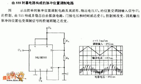
The pulse position modulating circuit composed of the 555 time-based circuit In the figure is the simple pulse position modulating circuit and its waveform. The position of the output voltage UA is controlled by the modulating input signal UE. The free oscillating circuit consists of 555, the gate voltage and the time delay is controlled by UE, so the position of the output pulse is changed by the control of the modulating signal.
(View)
View full Circuit Diagram | Comments | Reading(455)
The circuit of a watchdog
Published:2011/6/27 22:47:00 Author:Borg | Keyword: watchdog

See as the above figure: when the circuit is working, just send CD4060 the reset pulse timely, the Q1 will be blocked, so the NMOS pipe under control is conducting and provides with power for the processor circuit. The virtue of the circuit is that the timing-span is long, which can be several minutes, so it can offer enough time to the systems whose reset time is long. With the pulse feeding the watchdog, when the power is getting through, the counter is offered with a reset pulse by R2, C1 and R3, so Vout is made sure to have output. (View)
View full Circuit Diagram | Comments | Reading(654)
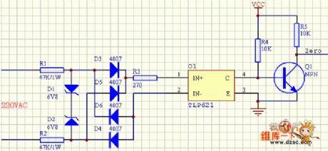
The zero passage circuit (experiment approved)
Published:2011/6/28 0:41:00 Author:Borg | Keyword: zero passage
View full Circuit Diagram | Comments | Reading(543)
The MacsotMR700 wireless microphone circuit
Published:2011/6/28 0:24:00 Author:Borg | Keyword: wireless microphone

View full Circuit Diagram | Comments | Reading(2410)
The DC servo separator amplifier circuit of photoelectric coupler
Published:2011/6/28 0:59:00 Author:Borg | Keyword: DC servo, amplifier, photoelectric coupler

In the figure is the DC servo separator amplifier of photoelectric coupler. This circuit is transmitting DC signals in the servo way, which has a feedback loop, so the high stabilization is got. VT1 and so on compose a constant circuit, which drives the LED in the photoelectric coupler hp-2731, and offers the bias current of 4mA when the signal is 0. Hp-2731 is the double photoelectric coupler, which has the tracking function, to make the circuit stable, what needs to be make sure is that the current in each LED is equal. A2 is the differential amplifier.
(View)
View full Circuit Diagram | Comments | Reading(1031)
CF155 Double-Power High Input-Impedance Single-Supply Amplifier Circuit Diagram
Published:2011/6/26 9:22:00 Author:Vicky | Keyword: Double-Power High Input-Impedance Single-Supply
CF155 series operational amplifier’s output circuit is composed by MOSFET. Its features are: low input current, low power supply current, low power dissipation, low noise, low offset voltage, and exterior zero-setting end. It is available in high-speed integrator, sampling/maintaining circuit of quick-speed D/A converter. The analog types or substitutions are: CFl55MT、CF255LT、CF355CT、CFl55MD、CF255LD、CF355CD、CFl55MJ、CF255LJ、CF355CJ、CF355CP. The above pictures are CF155 typical applied circuit: picture(a) is inverting amplifying and zero-setting circuit, and picture(b) is differential input and zero-setting circuit. (View)
View full Circuit Diagram | Comments | Reading(643)
AN7178 dual-channel power amplifier integrated circuit
Published:2011/6/28 7:47:00 Author:Christina | Keyword: dual-channel, power amplifier, integrated circuit


The AN7178 is designed as one kind of dual-channel power amplifier integrated circuit that is produced by the Panasonic company, it can be used in the Home audio equipments and the car audio equipments.
1.Features
The AN7178 has two channels of audio power amplifier circuit with the same function, and it has the over-voltage protection and overheating protection circuit. The features of this device are less external components, small distortion and the heat sink is easy to install. The internal circuit block diagram of the AN7178 is as shown in figure 1.
Figure 1. The internal circuit block diagram of the AN7178
2.Pin functions and data
The AN7178 uses the 12-pin single row package, the pin functions and data is as shown in table 1.
Table 1 The pin functions and data of the AN7178
3. The typical application circuit
Figure 2. The typical application circuit of the AN7178
(View)
View full Circuit Diagram | Comments | Reading(2941)
AN7168 duan-channel power amplifier integrated circuit
Published:2011/6/28 7:56:00 Author:Christina | Keyword: duan-channel, power amplifier, integrated circuit


The AN7168 is designed as one kind of dual-channel power amplifier integrated circuit that is produced by the Panasonic company, it can be used in the Home audio equipments and the car audio equipments.
1.Features
The AN7168 has the over-voltage protection circuit, the over-current protection circuit, the over-temperature protection circuit and two channels of audio amplifier circuits, it has the features of low distortion, small power supply switching noise and less external components. The internal circuit block diagram is as shown in figure 1.
Figure 1 The internal circuit block diagram of the AN7168
2.Pin functions and data
The AN7168 uses the 12-pin single row package, the pin functions and data is as shown in table 1.
Table 1 The pin functions and data of the AN7168
3. The typical application circuit
Figure 2 The typical application circuit of the AN7168
(View)
View full Circuit Diagram | Comments | Reading(1597)
AN7147N duan-channel power amplifier integrated circuit
Published:2011/6/28 8:04:00 Author:Christina | Keyword: duan-channel, power amplifier, integrated circuit

The AN7147N is designed as one kind of duan-channel power amplifier integrated circuit that is produced by the Panasonic company, and it can be used in the large screen color TVs which uses the Panasonic movements.
1.Features
The AN7147N is composed of two channels of audio power amplifier circuit with the same function, the overheating and short circuit protection circuit and other auxiliary function circuits. The output power of every sound channel is about 12.5W.
2.Pin functions and data
The AN7147N uses the 12-pin single row DIP package, the pin functions and data are as shown in table 1.
Table 1 The pin functions and data of the AN7147N
(View)
View full Circuit Diagram | Comments | Reading(1297)
AN7124 duan-channel power amplifier integrated circuit
Published:2011/6/29 1:02:00 Author:Christina | Keyword: duan-channel, power amplifier, integrated circuit

The AN7124 duan-channel power amplifier integrated circuit is produced by the Panasonic company that can be used in the large screen color TVs that use the Panasonic series machine.
1.Features
The AN7124 is composed of the two channels of power amplifier circuits with the same function, the standby control circuit, the static noise control circuit and the over-temperature and short circuit protection circuit.etc. The output power of the single track is about 15W.
2.Pin functions and data
The AN7124 uses the 12-pin single dual DIP package, the pin functions and data are as shown in table 1.
Table 1 The pin functions and data of the AN7124
(View)
View full Circuit Diagram | Comments | Reading(722)
AN6367NS chrominance signal processing integrated circuit
Published:2011/6/29 1:18:00 Author:Christina | Keyword: chrominance signal, processing integrated circuit


The AN6367NS chrominance signal processing integrated circuit is produced by the Panasonic company that can be used in the Panasonic NV-M series cameras.
1.Features
The internal main function of the AN6367NS is to produce the 5.06MHz signal by the vice converter, and supply the record and playback chromaticity signal transformation for the main converter, also it has the automatic frequency phase control function during the recording. The internal circuit block diagram of the AN6367NS is as shown in figure 1.
2.Pin functions and data
The AN6367NS is in the 22-pin dual-row plastic structure, the pin functions and data are as shown in table 1.
Table 1 The pin functions and data of the AN6367NS
3.The typical application circuit
The typical application circuit of the AN6367NS is as shown in figure 1.
Figure 1 The typical application circuit of the AN6367NS
(View)
View full Circuit Diagram | Comments | Reading(429)
AN6363AS chrominance signal processing integrated circuit
Published:2011/6/29 1:30:00 Author:Christina | Keyword: chrominance signal, processing integrated circuit


The AN6363AS chrominance signal processing integrated circuit is produced by the Panasonic company that can be used in the Panasonic NVM series cameras.
1.Features
The internal main function of the AN6363AS is to produce the interval phase line-by-line phase shifting 90°627KHz signal by the rotator, and the automatic frequency control of the time base correction circuit. The internal circuit block diagram of the AN6363AS is as shown in figure 1.
Figure 1 The internal circuit block diagram of the AN6363AS
2.Pin functions and data
The AN6363AS is in the 18-pin dual-row plastic structure, the pin functions and data are as shown in table 1.
Table 1 The pin functions and data of the AN6363AS
3.The typical application circuit
The typical application circuit of the AN6363AS is as shown in figure 1. (View)
View full Circuit Diagram | Comments | Reading(421)
AN5858K TV/AV switching control integrated circuit
Published:2011/6/29 2:11:00 Author:Christina | Keyword: TV/AV, switching control, integrated circuit


The AN5858K is designed as one kind of multi-channel electronic switch integrated circuit that can be used in the audio and video signal switching applications such as the large screen color TVs.
1.Internal circuit block diagram
The AN5858K has 4 channels of selector switch circuit, the internal circuit block diagram is as shown in figure 1.
Figure 1 The internal circuit block diagram of the AN5858K
2.Pin functions and data
The AN5858K uses the 42-pin dual-row DIP package, the pin functions and data are as shown in table 1.
Table 1 The pin functions and data of the AN5858K
(View)
View full Circuit Diagram | Comments | Reading(1427)
| Pages:1671/2234 At 2016611662166316641665166616671668166916701671167216731674167516761677167816791680Under 20 |
Circuit Categories
power supply circuit
Amplifier Circuit
Basic Circuit
LED and Light Circuit
Sensor Circuit
Signal Processing
Electrical Equipment Circuit
Control Circuit
Remote Control Circuit
A/D-D/A Converter Circuit
Audio Circuit
Measuring and Test Circuit
Communication Circuit
Computer-Related Circuit
555 Circuit
Automotive Circuit
Repairing Circuit