
Circuit Diagram
Index 1672
3DU series silicon phototransistor package type and dimension circuit
Published:2011/6/28 6:45:00 Author:Christina | Keyword: 3DU series, silicon phototransistor, package type, dimension circuit

The 3DU series silicon phototransistor can be used in the nearing infrared detector circuit, the optical coupling circuit, the encoder circuit, the characteristic identification circuit, the process control circuit and the laser receiving circuit.etc. The package type and dimension of it are as shown in the figure.
Figure The3DU series silicon phototransistor package type and dimension circuit (View)
View full Circuit Diagram | Comments | Reading(947)
Infrared detector circuit
Published:2011/6/28 3:09:00 Author:Christina | Keyword: Infrared detector

The infrared detector circuit can be used to detect whether the infrared remote control transmitter device is working properly. The infrared detector circuit is as shown in the figure. When the infrared remote control transmitter outputs the infrared light to irradiate the photosensitive transistor VT1, the resistance decreases to drive the conduction of VT2, so the light-emitting diode VD1 is lighted with the rhythm of the incident light. Because the brightness of the light-emitting diode VD1 depends on the intensity of the infrared light, so we can estimate that whether you can continue to use the battery.
Figure Infrared detector circuit (View)
View full Circuit Diagram | Comments | Reading(679)
Circuit Diagram of Power Frequency Detector composed of CD4013
Published:2011/6/21 6:09:00 Author:Vicky | Keyword: Power Frequency Detector

As so some electronic devices and electric apparatus, the frequency of AC power should meet a certain requirement. When the power supply is higher or lower than 50 Hz, the devices’/apparatus’ performance would be influenced, and even destroyed. Therefore, power frequency detector should be assembled for those devices/apparatus. When the power supply is not within required range of variation, the detector will give out warning or cut off the power supply automatically to ensure the security of the devices/apparatus. The above picture is power frequency detector composed of CD4013, which will cut off the working power when the power frequency is beyond a certain range around 50Hz to ensure the security of devices/apparatus. (View)
View full Circuit Diagram | Comments | Reading(2123)
AN5612 chromatic aberration/fundamental color conversion integrated circuit
Published:2011/6/29 2:28:00 Author:Christina | Keyword: chromatic aberration, fundamental color, conversion, integrated circuit


The AN5612 chromatic aberration/fundamental color conversion integrated circuit is produced by the Panasonic company that can be used in the large screen and picture in picture color TVs such as the ChangHong NC-3 series color TVs.
1.Features
The AN5612 has the functions of video signal amplification, chromatic aberration signal amplification and the G-Y signal matrix. The pin-2 of this IC is connected with the control regulating components to improve the video signal at the frequency of 2~3MHz. In addition, the line & field blanking pulse has the function of color signal blanking. The internal circuit block diagram is as shown in figure 1.
2.Pin functions and data
The AN5612 uses the 18-pin dual-row package, the pin functions and data are as shown in table 1.
Figure 1 The internal circuit block diagram
Table 1 The pin functions and data of the AN5612
3.The typical application circuit
The typical application circuit of the AN5612 is as shown in figure 2.
(View)
View full Circuit Diagram | Comments | Reading(1022)
Phototransistor circuit
Published:2011/6/29 2:47:00 Author:Christina | Keyword: Phototransistor

If you connect the phototransistor in this circuit, the collector of the phototransistor is connected with the positive potential, the emitter of it is connected with the negative potential. When there is no light irradiation, the current which flows through the phototransistor is the Iceo between the electrode and the emitter of the phototransistor, it is the dark current of the phototransistor: Iceo=(l+hFE)Icbo.
In this formula:
Lcbo--the saturated current between the collector electrode and base electrode;hFE--the DC amplification coefficient of the common-emitter.
The phototransistor has the higher sensitivity than the photosensitive diode.
(View)
View full Circuit Diagram | Comments | Reading(1563)
AN5421 line same-frequency signal detection integrated circuit
Published:2011/6/29 3:06:00 Author:Christina | Keyword: line, same-frequency signal, detection, integrated circuit


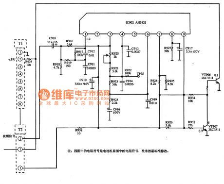
The AN5421 line same-frequency signal detection integrated circuit is produced by the Panasonic company that can be used in the Panasonic series large screen color TVs.
1.Features
The AN5421 can be used to detect the line synchronous signal from the frequency signal, and it outputs the detection result in the form of DC voltage to control the station search program of the system control microcomputer.
2.Pin functions and data
The AN5421 uses the single row 9-pin package, the pin functions and data are as shown in table 1.
Table 1 The pin functions and data of the AN5421
3. The internal circuit block diagram and the typical application circuit
The internal circuit block diagram of the AN5421 is as shown in figure 1, the typical application circuit is as shown in figure 2.
Figure 1 The internal circuit block diagram of the AN5421
Figure 2 The typical application circuit of the AN5421
(View)
View full Circuit Diagram | Comments | Reading(1466)
Phototransistor chip structure schematic circuit
Published:2011/6/29 3:26:00 Author:Christina | Keyword: Phototransistor, chip structure, schematic circuit

The phototransistor is the same as the conventional semiconductor transistor. It is the semiconductor tube that has the NPN or PNP structure with the semiconductor technology. The structure of it is similar with the semiconductor - diode, the extraction electrode of it is only one or two.
The phototransistor structure is as shown in the figure. In order to adapt to the requirements of the photoelectric conversion, the base region area is large, the launch region area is small. The incident light is mainly absorbed by the base region. The same with the phototransistor, the chips of the tube are installed in the metal shell, the light irradiates on the chips through the lens.
Figure: The Phototransistor chip structure schematic circuit (View)
View full Circuit Diagram | Comments | Reading(1031)
AN5342K picture definition enhancing integrated circuit
Published:2011/6/29 3:46:00 Author:Christina | Keyword: picture, definition, enhancing, integrated circuit


The AN5342K is designed as one kind of picture definition enhancing integrated circuit that is produced by the Panasonic company, and it can be used in the domestic and imported large screen color TVs.
1.Features
The AN5342K is composed of the full wave rectifier cutting circuit, the wave detection controller circuit, the brightness detection circuit, the one-time differentiator circuit, the gain control circuit, the details gain control circuit, the summator, the limiter, the second-time differentiator and other auxiliary circuits. The internal circuit block diagram of the AN5342K is as shown in figure 1.
Figure 1 The internal circuit block diagram of the AN5342K
2.Pin functions and data
The AN5342K uses the 30-pin dual-row DIP plastic package, the pin functions and data are as shown in table 1.
Table 1 The pin functions and data of the AN5342K
(View)
View full Circuit Diagram | Comments | Reading(635)
Multi-Channel Voltage Patrol Detecting(NE555,CD4066) Circuit Diagram
Published:2011/6/21 6:15:00 Author:Vicky | Keyword: Multi-Channel Voltage Patrol Detecting
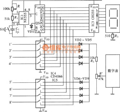
View full Circuit Diagram | Comments | Reading(3228)
Circuit Diagram of Frequency Shift Demodulator Composed of CA3020 and MC723
Published:2011/6/21 6:26:00 Author:Vicky | Keyword: Frequency Shift Demodulator
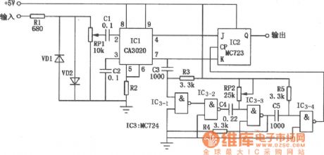
IC1 is a broadband amplifier CA3020 which constitutes input stage of circuit. It’s differential out is connected to input ends J &K of IC2 (JK trigger MC723). Gate circuit IC3 constitutes monostable multivibrator, with a timing cycle equaling with 1/2 center frequency cycle. The input signal will strobe the trigger after going through monostable multivibrator. For example, If 2920Hz represents symbol and 2750Hz represents blank space, then the center frequency is 2835Hz, therefore the cycle of monostable multivibrator is 175μs. When the input signal is 2920Hz, and the trigger strobe end is J=1, and K=0, then the Q end’s output is 1”1” (representing symbole); when the input signal is 2750Hz, and the trigger strobe is J=0 and K=1, then the Q end’s output is “0” (representing space). The detection accuracy of the circuit is determined by the timing accuracy of monostable multivibrator multivibrator. (View)
View full Circuit Diagram | Comments | Reading(652)
555 fridge automatic temperature controller circuit
Published:2011/6/16 2:31:00 Author:TaoXi | Keyword: 555, fridge, automatic, temperature controller
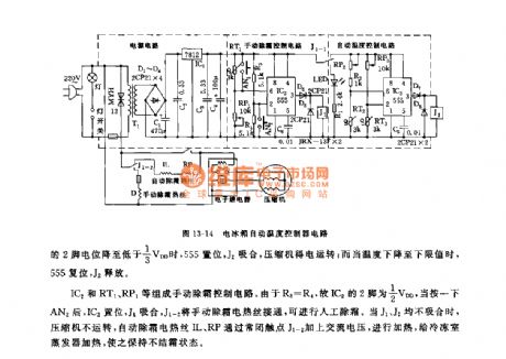
As the figure 13-14 shows, the fridge automatic temperature controller circuit is composed of the step-down voltage-stabilizing circuit, the automatic temperature control circuit, the manual defrosting control circuit and the relay control circuit. This circuit has all functions of the Toshiba GR204E automatic defrosting type automatic temperature control circuit.
The step-down voltage-stabilizing circuit is the +12V voltage source of the controller. The IC3(555) is connected into the bistable operating mode, the maximum temperature detection circuit is composed of the RP3 and RT3, the minimun temperature detection circuit is composed of the RP2,R2 and RT2, the RT2 and RT3 use the NTC negative temperature coefficient thermistor. When the temperature of fridge increases, the resistance of RT reduces.
(View)
View full Circuit Diagram | Comments | Reading(1199)
555 stereo audio equipment remote controller circuit
Published:2011/6/15 18:55:00 Author:TaoXi | Keyword: 555, stereo, audio equipment, remote controller
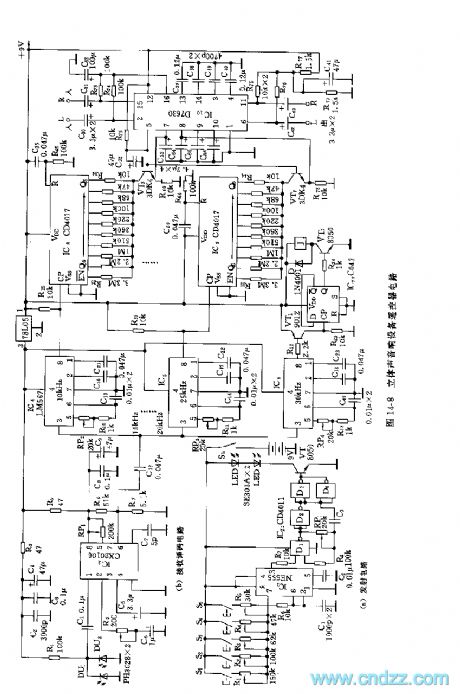
As the figure 14-8 shows, the remote controller is composed of the infrared ray coding emitter and the infrared ray decoding receiver. Figure (a) shows the 5-channel infrared coding emitter circuit. The astable multivibrator is composed of the 555 and C1, R6, R1 ~ R5, the oscillation frequency f=1.44/(R1-5+2R6)C1, the five channels are 10kHz,15kHz,20kHz,25kHz and 30kHz. The IC2 is the quad 2-input port NAND gate, the controlled oscillator is composed of the D1 and D2, the oscillation frequency f0=1/(1.4~2.2)RP1C3, f0 of the figure is about 38 to 40kHz. The infrared ray transmitting tube uses the SE303A or the HG4100 series tube. The receiver decoding circuit is composed of the infrared receiver tube, the special decoding circuit, the 5-channel single-tone decoder, the counting circuit and the stereo control circuit.etc.
(View)
View full Circuit Diagram | Comments | Reading(1066)
555 sound and light simultaneous display stress electronic metronome circuit
Published:2011/6/15 9:52:00 Author:TaoXi | Keyword: 555, sound, light, simultaneous display, stress, electronic metronome
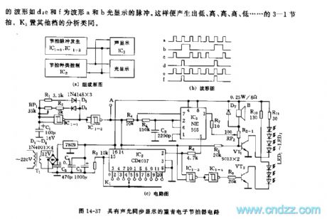
The stress electronic metronome is composed of the beat pulse generator, the beat type controller and the sound & light circuit, as the figure 14-37(a) shows, figure (b) is the waveform of all levels, figure (c) is the circuit. This metronome has 1-10 ten kinds of beat ways, the beat speed is 40-208 times/minute.
The IC1-1(1/4CD4093) quad 2 input Schmitt trigger is connected as the beat pulse oscillator, the positive pulse width is 100ms, RP1 can be used to change the pulse interval. The IC2(CD4017) is the 1-10 circulation counter, the cycling time is set by K1. In this figure, K1 is in the position of 4 , the waveform b is the output pulse of it. The IC3(555) is under the action of the waveforms a and b to output the high tone sound waveform such as c.
(View)
View full Circuit Diagram | Comments | Reading(1140)
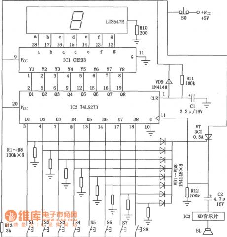
Circuit Diagram of Eight-Way Answer Device composed of CH233 and 74LS273
Published:2011/6/25 10:39:00 Author:Vicky | Keyword: Eight-Way Answer Device
View full Circuit Diagram | Comments | Reading(1144)
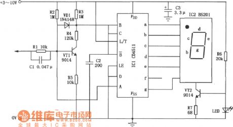
Circuit Diagram of Four-State Logic Displaying Pen composed of CD4511
Published:2011/6/25 10:40:00 Author:Vicky | Keyword: Four-State Logic Displaying Pen
View full Circuit Diagram | Comments | Reading(3808)
Circuit Diagram of Week Digital Dispaly composed of CH233 and CD4017
Published:2011/6/26 8:08:00 Author:Vicky | Keyword: Week Digital Dispaly
View full Circuit Diagram | Comments | Reading(405)
555 sound and light synchronous touch-bell metronome circuit
Published:2011/6/15 8:57:00 Author:TaoXi | Keyword: 555, sound, light, synchronous touch-bell, metronome
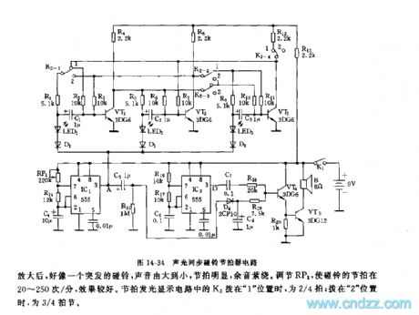
As the figure 14-34 shows, the metronome is composed of two beat generators, the bell sound amplification circuit and the luminous display circuit.
The multivibrators is composed of the IC1, RP1, R14, C4 and the IC2, R16, R17, C6 respectively, the oscillation frequency of IC1 is f1=1.44/(RP1+2R14)C4, it is in the range of 1Hz~100Hz. The oscillation frequency of IC2 is f2=1.44/(R16+2R17)C6, it is about 1000Hz. The duty ratio of IC1's oscillation square-wave can be very large, if the resistance of RP1 is 100kΩ, f1 is about 2Hz, the duty ratio is about 99%.
The oscillation square-wave which is output by the IC2 adds to VT4 through C7 and R18. When the positive differential pulse of IC1 comes, the two channels of signals act on VT4 at the same time to make the jet current of VT4 very large.
(View)
View full Circuit Diagram | Comments | Reading(933)
Road Night Auto Electronic Guidepost Circuit Diagram
Published:2011/6/21 6:45:00 Author:Vicky | Keyword: Road Night Auto Electronic Guidepost
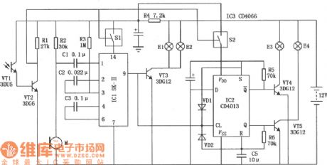
Auto electronic guidepost’ circuit diagtam is shown as in the picture. When night falls, the indicator light E3 gives out red light, warning that the section is dangerous. When there is vehicle getting close to the dangerous section, the traffic sign composed of indicator lights E1 and E2 is shown and meanwhile indicator E3 and E4 sparkle, giving out red and green light respectively. When the vehicle drives away, the indicator E3 keeps giving out red light, while indicator E1, E2 and E4 go out. The circuit is mainly composed of sound-control circuit, oscillating circuit and display driving circuit etc. (View)
View full Circuit Diagram | Comments | Reading(960)
555 sound and light signal metronome circuit
Published:2011/6/15 8:38:00 Author:TaoXi | Keyword: 555, sound, light, signal, metronome
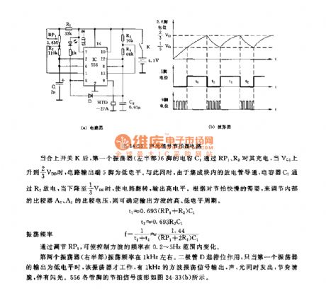
As the figure 14-33 shows, this circuit is composed of a pair of time base circuit 556, and the two time base circuits are connected into two multivibrators. One multivibrator is used to produce the 1kHz oscillation square-wave, this oscillation square-wave is output from pin-9 to encourage the piezoelectric ceramics to send out the sound. Another multivibrator is used to produce the low frequency square-wave to modulate the 1kHz square-wave signal.
After the switch K is closed, pin-6's capacitance C1 of the first oscillator charges it through RP1, when the voltage of VC1 is 2/3VDD, the circuit's output port pin-5 has the low electrical level. At the same time, because the disrharge tube of the integrated block is conducted, so the capacitor C1 charges through R2, when the voltage of C1 is 1/3VDD, the circuit turns to output the high electrical level.
(View)
View full Circuit Diagram | Comments | Reading(740)
555 ten notes continuous playing circuit
Published:2011/6/15 8:11:00 Author:TaoXi | Keyword: 555, ten notes, continuous playing
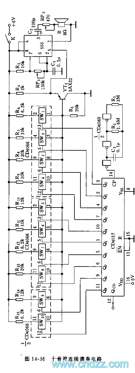
As the figure 14-36 shows,the frequency controllable multivibrator is composed of the 555 time-base circuit and some capacitance resistance components. The control port pin-5 of 555 is connected with the output port of the launch follower VT1, and the VT1 is controlled by the time sequence switching circuit to make the 555 to produce the ten notes of 6 1 3 1 2 1 7 3 2 6.
The oscillator which has the period of 0.6s is composed of the CMOS six phase-inverter CD4069 and three gate circuits, the notes add to the time sequence distributor which is composed of the decimal counter CD4017 to make the 10 output ports of it controls the four two-way switch circuit CD4066 respectively, and these switches turn on one by one and it adds to the base electrode of the emitter-follower VT1.
(View)
View full Circuit Diagram | Comments | Reading(465)
| Pages:1672/2234 At 2016611662166316641665166616671668166916701671167216731674167516761677167816791680Under 20 |
Circuit Categories
power supply circuit
Amplifier Circuit
Basic Circuit
LED and Light Circuit
Sensor Circuit
Signal Processing
Electrical Equipment Circuit
Control Circuit
Remote Control Circuit
A/D-D/A Converter Circuit
Audio Circuit
Measuring and Test Circuit
Communication Circuit
Computer-Related Circuit
555 Circuit
Automotive Circuit
Repairing Circuit