
Circuit Diagram
Index 1681
band-pass filter formed by the low-pass and high pass filters in series circuit
Published:2011/6/20 6:04:00 Author:John | Keyword: band-pass filter, high pass filter

Band-pass filter is used to allow -3dB cutoff frequency with the low end and the high end. The frequency out of this range is eliminated. A simple way to get band-pass frequency’s response is to design a band-pass filter formed by the low-pass and high pass filters in series (as shown). And the cutoff frequency of HPF is designed to be equal to the cutoff frequency on the low end of the band-pass filter. Component values are calculated by the separate parts respectively.
(View)
View full Circuit Diagram | Comments | Reading(749)
Simple gradually dark/light switch circuit (2)
Published:2011/6/27 22:23:00 Author:Ecco | Keyword: Simple , gradually dark, light, switch

View full Circuit Diagram | Comments | Reading(795)
Ⅱtype low-pass filter with three component circuit
Published:2011/6/20 5:51:00 Author:John | Keyword: low-pass filter

Ⅱtype low-pass filter with three component circuitis shown.
(View)
View full Circuit Diagram | Comments | Reading(709)
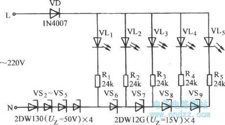
The intensity-scale of electronic touch dimmer incandescent
Published:2011/6/27 4:18:00 Author:Ecco | Keyword: intensity-scale , electronic, touch , dimmer incandescent

View full Circuit Diagram | Comments | Reading(1311)
Voltage monitor circuit
Published:2011/6/27 4:27:00 Author:Ecco | Keyword: Voltage , monitor circuit
View full Circuit Diagram | Comments | Reading(552)
TV control automatic light circuit
Published:2011/6/27 4:34:00 Author:Ecco | Keyword: TV , control , automatic light

Watching TV requires certain brightness around, or a long time watching TV is not conducive to protect eyes. The circuit shown as the chart is the background small lamps lighting circuit controlled by TV. When the TV is turned on, the small lamps will be automatically lit, When the TV is turned off, the lights can automatically turned off, while watching TV during the day, the lights will be blocked and not be lit up automatically. The electromagnetic coil L need to be self-made, you should find the input or output transformer core in an old radio, and cut one side of the coil, the core will change into a U shape.
(View)
View full Circuit Diagram | Comments | Reading(639)
Photoelectric photometry switch circuit diagram
Published:2011/6/27 4:56:00 Author:Ecco | Keyword: Photoelectric, photometry, switch
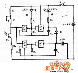
After the power switch K is turned on, beat pulse generator and audio oscillator pulse will begin to work. In the part of beat pulse generator, YF1 and YF2 output pulses have opposite polarity. With the output of oscillator pulse, light emitting diodes LED1 and LED2 alternately emit light, and the flash cycle is determined by R3, C1 values; in the part of audio oscillator, the oscillation voltage is determined by the output end of YF4, then HTD issues single-frequency sound, and the audio pulse frequency is established by the R7, C2 values.
(View)
View full Circuit Diagram | Comments | Reading(455)
Integrated regulated power supply circuit diagram
Published:2011/6/27 5:00:00 Author:Ecco | Keyword: Integrated , regulated , power supply

This is a continuously adjustable output voltage integrated power supply, and the output voltage is continuously adjustable between 1.25-37V, and the maximum output current is up to 1.5A. Circuit is simple and suitable for self-made by electronic lovers. It can be used for a variety of small electrical power supply. LM317 output current is 1.5A, the output voltage can be adjusted continuously between 1.25-37V, and the output voltage is set by two external resistors R1, RP1, and the voltage difference between the output end and adjusting end is 1.25V, and the voltage will produce a few milliamps of current.
(View)
View full Circuit Diagram | Comments | Reading(609)
The human body sensor lights with LM358 designing
Published:2011/6/27 5:07:00 Author:Ecco | Keyword: human body, sensor lights , designing


The infrared sensors, signal amplifier circuit, voltage comparator, delay circuit and sound alarm circuit form the human body sensor lights with LM358 designing. IC1 infrared detection sensor can detect the infrared radiation signals in front of the body, and the output pin ② of IC1 outputs weak electrical signals, which is amplified by the first-class amplification circuit composed of transistor VT1, then input to the op-amp IC2 and done the high-gain, low-noise amplified, then this time the pin ① of IC2 outputs enough strong signals. IC3 is used as a voltage comparator.
(View)
View full Circuit Diagram | Comments | Reading(4080)
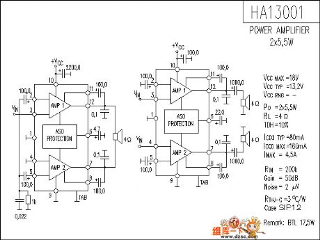
HA13001 audio IC circuit diagram
Published:2011/6/27 5:12:00 Author:Ecco | Keyword: audio, IC circuit
View full Circuit Diagram | Comments | Reading(2254)
The typical application circuit diagram of nRF401
Published:2011/6/27 5:12:00 Author:Ecco | Keyword: typical application
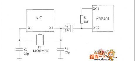
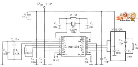
UDD uses +3 V supply. The R1, JT, C1 and C2 constitute the crystal circuit, and C3, C4 and R2 form the loop filter. R3 is the power set resistor. C5 is the power supply decoupling capacitor; C6 and C7 are noise reduction capacitors. DIN, DOUT terminals are respectively connected MCU TXD (serial output), RXD (serial input) sides. To simplify the circuit, nRF401 μC can be combined with a crystal oscillator circuit, the circuit is shown as below. X1, X2 are respectively μC crystal input end and output end, the resulting crystal frequency is directly sent to the XC2 side of nRF401.
(View)
View full Circuit Diagram | Comments | Reading(467)
Infrared remote control energy-saving lamp circuit diagram
Published:2011/6/27 3:53:00 Author:Ecco | Keyword: Infrared, remote control, energy-saving lamp

View full Circuit Diagram | Comments | Reading(2158)
Relay control circuit diagram
Published:2011/6/27 3:52:00 Author:Ecco | Keyword: Relay , control

View full Circuit Diagram | Comments | Reading(436)
High-efficiency 70W universal switching power supply module circuit diagram
Published:2011/6/27 4:03:00 Author:Ecco | Keyword: High-efficiency , 70W , universal , switching power supply , module

TOPSwitch GX is suitable for making low-cost, high efficiency, small size, full-enclosed switching power supply module or power adapter (adapter). When the ambient temperature does not exceed 40 ℃, the module can be reduced to the dimensions of 10.5mm × 5.5mm × 2.5mm. The AC input voltage range is 85V ~ 265V, which is a common worldwide voltage range. Rated output power is PO = 70W; load regulation is SI = ± 4%; power efficiency is η ≥ 84% (when the AC input voltage U = 85V, full load efficiency is 85%; when U = 230V, the power efficiency is up to 90% ); load power consumption is <0.52W (U = 230V pm).
(View)
View full Circuit Diagram | Comments | Reading(6121)
45 W multi-output switching power supply circuit diagram composed of TOP246Y
Published:2011/6/27 3:59:00 Author:Ecco | Keyword: 45 W , multi-output , switching, power supply

It can be used as set-top box, cable decoder, high-capacity hard disk drive or laptop computer switching power supply. The power supply input voltage is AC 185V ~ 265V, and the rated output power is 45W, and the peak output power is up to 60W; power efficiency is η ≥ 75%, no-load power consumption is only 0.6W. Five outputs are: UO1 (5V, 3.2A), UO2 (3.3V, 3A), UO3 (30V, 0.03A), UO4 (18V, 0.5A), UO5 (12V, 0.6A); their load regulation rates are ± 5%, ± 5%, ± 8%, ± 7%, ± 7%.
(View)
View full Circuit Diagram | Comments | Reading(4543)
Three-level passive lossless soft-switch PFC topology circuit
Published:2011/6/27 19:38:00 Author:John | Keyword: soft-switch

View full Circuit Diagram | Comments | Reading(1174)
the control circuit of the common electric motor(3)
Published:2011/6/25 20:40:00 Author:Ariel Wang | Keyword: control, common, electric motor

Now we will introduce the control circuit of electric motor which can both jog control and long-term operation.S1 is the start button.52 is the stop button.53 is jog control button.When it gets start, the knife switches get through.When 51 is pressed,KM is pulled in.The normally open contacts KM1 and KM2 are connected.The electric motor M starts to work.When 51 is disconnected,KM stays pull in as the contactor of KM2 is connected already.When you want to stop it,you can press 52.KM is released.The normally open contact is disconnected.M stops working.When you want to jog control it,you can press 53.KM is conducted to pull in.M starts to work.When 53 is disconnected.KM is released.M stops working.
(View)
View full Circuit Diagram | Comments | Reading(3135)
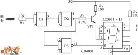
Text displaying logic pen 4 circuit diagram composed of gate circuit
Published:2011/6/27 3:55:00 Author:Ecco | Keyword: Text, displaying , logic pen , gate circuit
View full Circuit Diagram | Comments | Reading(428)
Tel indicator circuit
Published:2011/6/27 4:16:00 Author:Ecco | Keyword: Tel , indicator circuit

View full Circuit Diagram | Comments | Reading(597)
PFC lossless snubber main circuit
Published:2011/6/25 10:58:00 Author:John | Keyword: snubber

The charging process with normal charge mode is generally carried out in the home and public places. The normal charging mode’s charging power level is typically 6.6kW and its typical recharging time is 5 to 8 hours. The power converter of the normal charging mode is similar to that of the emergency charging mode. Normal charging mode also can use a single-stage AC / DC converter. However, with the single-stage PFC converter, the peak current of the switching tube is large. In the two converters, PFC Boost level can use to traditional Boost lifting circuit. The switch can be soft switch or hard switch.
(View)
View full Circuit Diagram | Comments | Reading(1662)
| Pages:1681/2234 At 2016811682168316841685168616871688168916901691169216931694169516961697169816991700Under 20 |
Circuit Categories
power supply circuit
Amplifier Circuit
Basic Circuit
LED and Light Circuit
Sensor Circuit
Signal Processing
Electrical Equipment Circuit
Control Circuit
Remote Control Circuit
A/D-D/A Converter Circuit
Audio Circuit
Measuring and Test Circuit
Communication Circuit
Computer-Related Circuit
555 Circuit
Automotive Circuit
Repairing Circuit