
Circuit Diagram
Index 1684
relay isolation circuit of DTL
Published:2011/6/15 7:16:00 Author:chopper | Keyword: relay, isolation circuit, DTL

In this circuit,geminate transistors can counteract and prevent from generating natural current.When DTL logical cicuit outputs 1 ,Q1 will be conducted and LED is no current.Q2 will close,relay K1 will sotp running.When the DTL outputs 0 ,Q1 will close,and there is current through LED.Q2 will be conducted,K1 wil run.Action time is relative to mechanical response characteristic of relay.
(View)
View full Circuit Diagram | Comments | Reading(621)
complementary symmetry principle circuit of power supply
Published:2011/6/11 5:13:00 Author:chopper | Keyword: complementary symmetry, principle, power supply

The picture 1 is a complementary symmetry principle of one power source circuit. T3 forms preamplifier stage,T1 and T2 form output stage of complementary symmetry circuit.Only the value of R1,R2 is necessary to make IC3,VB2 and V1 reach the required value when it is static.Provide T1 and T2 with a appropriate setover to make the electric potential VK=VCC/2.
(View)
View full Circuit Diagram | Comments | Reading(836)
LM393 nickel-cadmium battery charger circuit of high performance-price ratio
Published:2011/6/22 10:15:00 Author:chopper | Keyword: nickel-cadmium battery charger, high performance-price ratio

The LM393 nickel-cadmium battery charger circuit of high performance-price ratio is shown as the picture,it has the following features:(1)The process of constant-current charge runs with the process of heavy current discharge.The value of current of constant-current charge is about 300mA.And the discharge current increases along with the increase of battery voltage and the value of discharge current will reach 400mA when the battery is to the full value.The charging time is 1.5 second,discharging time is 0.5 second,and take turns. When the heavy current charge is over,there is about 5mA purling current charging.(2)The detection of battery voltage works during the discharging.It is because that the voltage of charge is greater than the discharge.
(View)
View full Circuit Diagram | Comments | Reading(3641)
Mode-6 counter circuit composed of the reset port and the preset port
Published:2011/6/20 1:58:00 Author:TaoXi | Keyword: Mode-6 counter, reset port, preset port
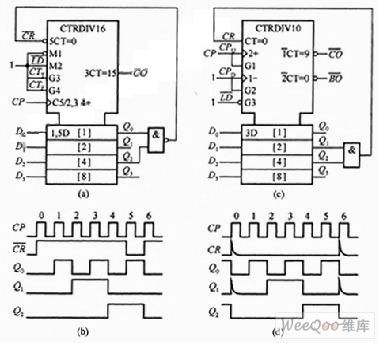
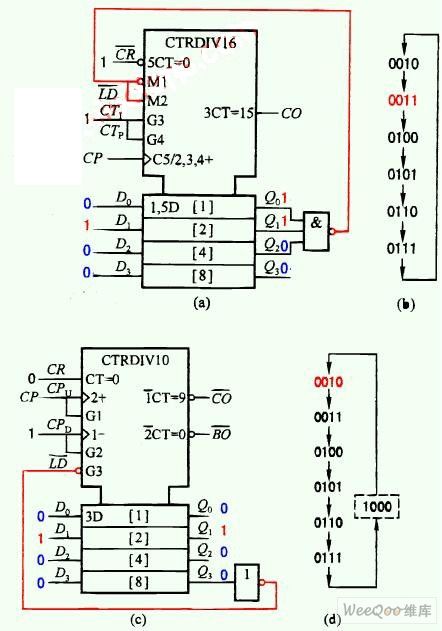
By using the reset port and the preset port of the counter, we can form the any-mode counter.
The figure shows the mode-6 counters which are composed of the 74163 and 74192, the operating waveform is as shown in the figure.
The mode-6 counter which is composed of the preset port (View)
View full Circuit Diagram | Comments | Reading(1611)
TA7668 integrated circuit with dual channels preposing of recording,playback
Published:2011/6/17 20:58:00 Author:chopper | Keyword: integrated circuit, dual channels, preposing, recording, playback

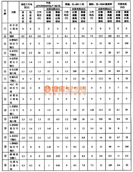
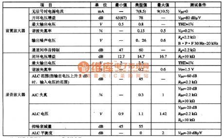
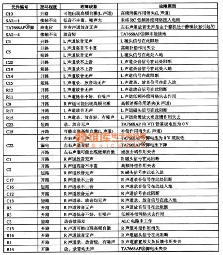
TA7668 is a typical integrated circuit with dual channels preposing of recording,playback.This IC is applied to sound system like walkman,radio-tape recorder,music center widely.1.the inner circuit and typical application of TA7668The inner circuit and typical application of TA7668 integrated package are shown as picture 1.The amplifiers of the record circuit are independent.IC includes automatic level control,noise elimination and other functional circuits besides two preamplifiers of same function and recording post-amplifier.
(View)
View full Circuit Diagram | Comments | Reading(2656)
MAX1757 lithium ion battery charger circuit
Published:2011/6/17 20:28:00 Author:chopper | Keyword: lithium ion, battery charger

MAX1757 is formed by power supply and charger.As to power supply,there are DC/DC step-down convertor and 5.4V linear voltage regulator.DC/DC convertor can charge the battery with constant current and voltage,and its maximum charge current can reach 1.5A.The typical application circuit of MAX1757 is shown as follows.
(View)
View full Circuit Diagram | Comments | Reading(1903)
acousto-optic logical pen circuit of NE555
Published:2011/6/17 6:44:00 Author:chopper | Keyword: acousto-optic, logical pen,

View full Circuit Diagram | Comments | Reading(652)
Interface circuit between the serial 12-bit ADC and the computer
Published:2011/6/20 2:13:00 Author:TaoXi | Keyword: Interface circuit, serial 12-bit ADC, computer

In recent years, the IC manufacturers design various methods to achieve the interface, and they pay special attention to reduce the I/O pin number of the IC interface. The MAX187 is such a device which is designed as the 12-bit D/A converter (ADC). You can use the serial data communication technology to produce a interface that matches the ADC. The A/D conversion and data transmission of the MAX187 only needs three digital I/O lines. You can use the PC's Centronics printer port to produce a simple interface between the MAX187 and PC (figure 1). As long as the pins are set to the high or low level, you can enable or disable the MAX187 (pin-3).
Figure 1 The interface between the 12-bit ADC and the PC (View)
View full Circuit Diagram | Comments | Reading(850)
2.75W constant voltage/constant current general input charger power supply circuit
Published:2011/6/20 2:39:00 Author:TaoXi | Keyword: 2.75W, constant voltage, constant current, general input charger, power supply

The 2.75W constant voltage/constant current general input charger power supply circuit is as shown in the figure, this design uses the Power Integrations's LinkSwitch series product LNK613DG. This design is very suitable for the cellphone or the USB charger applications such as the cell phone battery charger, the USB charger and the constant pressure/constant current applications.
In this design, the diodes D1-D4 rectify the AC input, the capacitance C1 and C2 filter the DC input. The π type filter is composed of the L1, C1 and C2 to attenuate the differential mode conduction EMI noises.
The RCD-R ground-clamp circuit is composed of the D5, R2, R3 and C3, it can be used to limit the drain voltage peak which is caused by the leakage inductance.
(View)
View full Circuit Diagram | Comments | Reading(877)
5W general input constant voltage/constant current charger power circuit
Published:2011/6/20 2:49:00 Author:TaoXi | Keyword: 5W, general input, constant voltage, constant current, charger, power circuit

The 5W general input constant voltage/constant current charger power circuit is as shown in the figure, this design uses the Power Integrations's LinkSwitch-II series product LNK-616PG. This design is very suitable for the cellphone or the USB charger applications such as the cell phone battery charger, the USB charger and the constant pressure/constant current applications.
As the response of the voltage droping of the pin-FB, the switch frequency will reduce too, so as to realize the linear constant current output. The RCD-R ground-clamp circuit is composed of the D5, R3, R4 and C3, it can be used to limit the drain voltage peak which is caused by the leakage inductance. The resistor R4 has large value to avoid the drain voltage waveform oscillation which is caused by the leakage inductance, this can improve the voltage stability and reduce the EMI generation.
(View)
View full Circuit Diagram | Comments | Reading(638)
Triangle wave and sine wave producing circuit
Published:2011/6/20 3:09:00 Author:TaoXi | Keyword: Triangle wave, sine wave, producing circuit
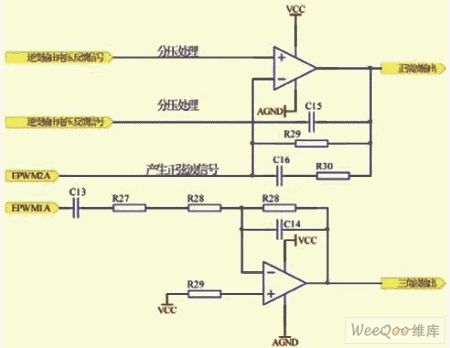
The input signal of the triangle wave producing circuit is from the EPWM1A's pin of the DSP, this signal is the PWM signal, it is integrated and changes into the triangle wave, then it is sent into the PWM producing circuit. The PWM signal which comes fron the TMS320F28335 is filtered by the second stage low-pass to produce the sine wave reference signal, this signal inverts with the inverter output voltage feedback signal. The PWM signal which is output by the pin of the EPWM2A is the city electricity input tracking signal, this circuit has the regulation function to the input sine wave signal. The figure shows the triangle wave and sine wave producing circuit.
(View)
View full Circuit Diagram | Comments | Reading(953)
current-limiting protection charger of CW117/CW217/CW317 circuit
Published:2011/6/16 0:46:00 Author:chopper | Keyword: current-limiting protection, charger

View full Circuit Diagram | Comments | Reading(1005)
STR-S6708 switching power supply thick film integrated circuit
Published:2011/6/15 7:33:00 Author:chopper | Keyword: switching power supply, thick film

STRS6708 is a mixed type switching power supply thick film integrated circuit (View)
View full Circuit Diagram | Comments | Reading(1229)
CAN bus communication circuit
Published:2011/6/20 3:17:00 Author:TaoXi | Keyword: CAN, bus, communication

CAN bus communication circuit (View)
View full Circuit Diagram | Comments | Reading(6538)
CAN interface circuit
Published:2011/6/20 3:11:00 Author:TaoXi | Keyword: CAN, interface circuit

CAN interface circuit (View)
View full Circuit Diagram | Comments | Reading(799)
the protection circuit of power circuit
Published:2011/6/11 21:10:00 Author:chopper | Keyword: protection circuit, power circuit

The current in power circuit is great and wecan adopts fuse,diode,transistor circuit to limit the current.Fuse is the simplest protection component.Picture a,b are the examples of setup method of fuse.The fuse is connected with the protection circuit and loads in series.Classify by fusing time,there are fast type,low type and normal type.We should select appropriate fuse based on the different loads and driving circuit.
(View)
View full Circuit Diagram | Comments | Reading(688)
ADC0809 interface circuit
Published:2011/6/20 3:23:00 Author:TaoXi | Keyword: interface circuit
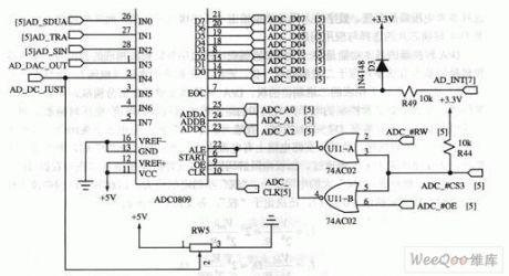
ADC0809 interface circuit (View)
View full Circuit Diagram | Comments | Reading(1309)
Four hours order timer circuit
Published:2011/6/20 3:39:00 Author:TaoXi | Keyword: Four hours, order timer

The four hours order timer circuit uses the N8281 distributor network between the two timers of the double timer 556, it does not use the big volume low leakage current capacitor, so it has the long delay time. The first timer forms the oscillator, the output adds to the output which is produced by the N frequency division network with the N/f cycle, it triggers the monostable circuit which is composed of the second timer. The delay time depends on the delay output time of the distributor. You can cascade some distributors to make the delay time to a few days or weeks.
(View)
View full Circuit Diagram | Comments | Reading(1012)
STR-S5708 switching power supply thick film integrated circuit
Published:2011/6/15 7:34:00 Author:chopper | Keyword: switching power supply, thick film

STRS5708 is a mixed type switching power supply thick film integrated circuit (View)
View full Circuit Diagram | Comments | Reading(656)
printed plate of switch power supply design technique circuit
Published:2011/6/11 22:01:00 Author:chopper | Keyword: printed plate, switch power supply

Switch power supply uses high speed switch to control high voltage and great current.If the speed of switch is not fast,the comsuption of transistor will increase and the temperature will ascend.When current changing rate di/dt is comparatively big,it will cause biggish noise voltage.When the inductance of line of printed plate is different,the switch waveform is different.The inductance of line is large,the surge of voltage waveform is large and the step gapof current waveform is large too.Therefor,the lines of switch current should be short and thick to decrease the inductance.
(View)
View full Circuit Diagram | Comments | Reading(753)
| Pages:1684/2234 At 2016811682168316841685168616871688168916901691169216931694169516961697169816991700Under 20 |
Circuit Categories
power supply circuit
Amplifier Circuit
Basic Circuit
LED and Light Circuit
Sensor Circuit
Signal Processing
Electrical Equipment Circuit
Control Circuit
Remote Control Circuit
A/D-D/A Converter Circuit
Audio Circuit
Measuring and Test Circuit
Communication Circuit
Computer-Related Circuit
555 Circuit
Automotive Circuit
Repairing Circuit