Circuit Diagram
Index 1692
Bart woz fourth-stage active low-pass filter circuit
Published:2011/6/23 21:27:00 Author:TaoXi | Keyword: Bart woz, fourth-stage, active, low-pass filter
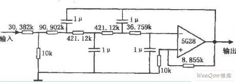
This device is designed as the Bart woz fourth-stage active low-pass filter circuit that can be used to filter the very low frequency random impulsive noise interference voltage of the DC level signal, the cut-off frequency (-3dB) is about 8Hz, the gain reduces 20dB when the frequency is 18Hz. The pass-band natural attenuation is 0.467. The input resistance is about 40kΩ. The filter network resistor is composed of some metal film precise resistance. If the 1μF capacitance has the good precision, the cut-off frequency fc closes to the theoretical value.
(View)
View full Circuit Diagram | Comments | Reading(531)
The Butterworth 4-stage switch capacitor low-pass filter (TLC04)
Published:2011/6/17 6:46:00 Author:Borg | Keyword: Butterworth, switch capacitor, low-pass filter

The filter circuit is shown in figure 5. The main part of the filter circuit consists of the Butterworth 4-stage switch capacitor low-pass filter (TLC04) which is produced by TI Corp., US, and the self-timing dual power supply of Schmidt trigger oscillator is the power supply. The stability of TLC04 blocking frequency is only related with the clock frequency stability, the blocking frequency clock is adjustable, the clock-blocking frequency ratio is 50:1, so the designed blocking frequency is 1/1.69×RF1×CF1×50=251.8Hz, which satisfies the requirements of oscillating aging and oscillating wielding technique.
(View)
View full Circuit Diagram | Comments | Reading(646)
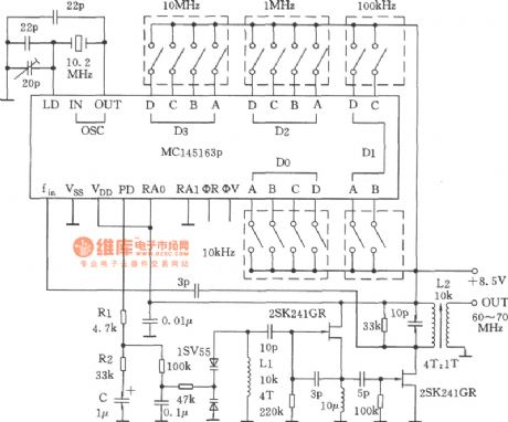
The 60~70MHz PLL frequency synthesizer circuit composed of MC145163P
Published:2011/6/17 6:55:00 Author:Borg | Keyword: frequency synthesizer, PLL
View full Circuit Diagram | Comments | Reading(3108)
The odd-even frequency splitter composed of SN74193
Published:2011/6/17 22:14:00 Author:Borg | Keyword: frequency splitter
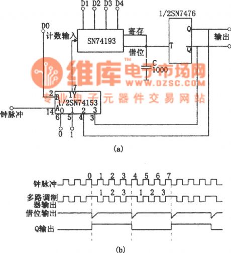
In the figure is the odd-even frequency splitter circuit. This circuit can engage in 2~32 (including odd and even) times of splitting. The counting input of the synchronized counter SN74193 is provided by the output 1Y of the multiplexer SN74153, the borrow output of the counter can not only drive the trigger SN7476, but also it's the deposit input pulse of SN74193. The 5-bit binary numbers are imposed on D0, D1, D3 and D4 input terminals, which decides the splitting constant(2~32), and D0 is the lowest bit. When D0=0, the outputting pulse phase of the multiplexer is determined according to the trigger state. (View)
View full Circuit Diagram | Comments | Reading(1251)
The digital frequency doubler(LM108 and LM111)
Published:2011/6/17 9:45:00 Author:Borg | Keyword: digital frequency doubler
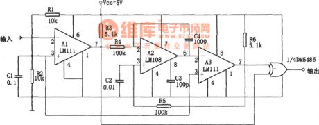
The circuit consists of the voltage comparator, Miller integrator and OR gate. A1 is the LEV comparator, which is fulfilled by the chip LM111, the chip forms the rectifier circuit that converts the long-rising-time waveform (such as the sine wave) to the short-rising-time square wave. The square wave output by A1 is turned into the triangular wave by the Miller integrator which consists of A2, R4 and C4, and then the LEV comparator A3 turns the triangular wave into the square wave. There is a 90⁰ phase difference between A1 and A3, so after crossing the the OR gate, the wave is doubled and then output. (View)
View full Circuit Diagram | Comments | Reading(662)
The frequency splitter of symmetric output waveforms (μL9020)
Published:2011/6/22 4:29:00 Author:Borg | Keyword: frequency splitter, symmetric output waveforms
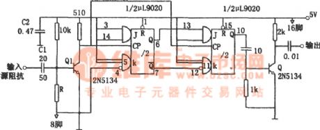
The figured splitter circuit is triggered when the peak value is in the range of 0.5~5v, no matter whether it is the sine wave or the square wave. The working frequency of the circuit is 40MHz. The input signal of the frequency splitter drives the J-K triggers after it has passed the amplitude limit amplifier Q1, finally, it crosses the buffer Q2 and is output. The transistor Q1 offers the first stage splitter a proper triggering LEV. When the high LEV drives, the capacitor C1 plays a part of current limitation. If the drive LEV is low, we can expand the volume of C1, the the trigger power is increased. (View)
View full Circuit Diagram | Comments | Reading(531)
The 4-time frequency circuit composed of CH7555
Published:2011/6/17 7:35:00 Author:Borg | Keyword: frequency circuit
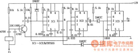
In the figure is the 4-time frequency circuit. This circuit consists of 3 CH7555 timers. When the symmetric wave is input, it is turned into the twice frequency by the phase inverter and the transistor. The two signals trigger the CH7555 single circuit at the same time, so that there generates two teams of pulses with different band widths on the output terminals of IC1 and IC2, then their dropping edges are to trigger the single stable circuit consisting of IC3, finally, a four-time frequency is generated on the output terminal of IC3. (View)
View full Circuit Diagram | Comments | Reading(441)
The frequency splitter composed of TTL decimal counter
Published:2011/6/22 2:21:00 Author:Borg | Keyword: frequency splitter, TTL decimal counter
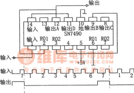
In the figure is the frequency splitter composed of TTL decimal counter. In many conditions, we need to do N spitting to the pulse sequence(N is an integral). For example, the digital clock needs 60 frequency splitting, so we get the pulses of 1Hz repeated frequencies; and also, the time standard generator needs to split the crystal oscillator output frequency. If the splitting parameter N≤10, then we only need a TTL binary-decimal counter SN7490. Usually, the frequency splitter of TTL circuits is a binary counter, which make every N input pulses launch a pulse. (View)
View full Circuit Diagram | Comments | Reading(637)
The frequency divider composed of R-S triggers (SN7442)
Published:2011/6/26 20:45:00 Author:Borg | Keyword: frequency divider, R-S triggers
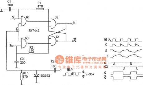
In the figure is the frequency divider composed of R-S triggers. The circuit can work in a wide frequency range and input pulse width. Compared with the standard R-S multi-resonance oscillator, the circuit must be stable after being improved. The integrator R1C1 and R2C2 form a feedback net, the integrating constant is selected according to the following formula: T<0.6RC, of which T is the width of the input pulse width. According to the above requirement, the NANDs of G1 and G2 won't output low LEVs at the same time. The working frequency of the circuit could be several MHz. (View)
View full Circuit Diagram | Comments | Reading(978)
The simple TV signal generator
Published:2011/6/17 22:35:00 Author:Borg | Keyword: signal generator
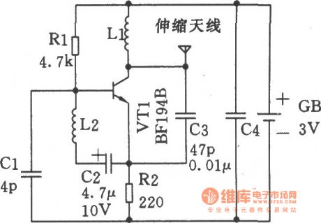
This generator can test if the TV receptor is good in 5 meters. See as the figure, the circuit is mainly a VFH oscillator, which consists of the triode BFI948 and the external components. The circuit can generate black-white stripe images on the TV screen and output an audio signal in the loudspeaker. The circuit only needs a 3V battery. In the circuit, both L1 and L2 use No.21 SWG high-intensity enameled wires to wind 8 turns around the hollow frame whose diameter is 5mm, by changing the value of the 4.7μF capacitor and the turns of L1 and L2, the number of the stripes and the sound frequency can be changed. (View)
View full Circuit Diagram | Comments | Reading(1172)
Infrared sensor high voltage dangerous voice warning circuit diagram
Published:2011/6/23 20:40:00 Author:Nicole | Keyword: infrared sensor, dangerous voice warning
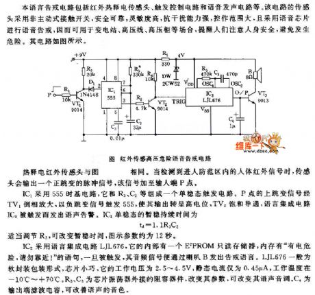
Pyroelectric infrared sensor head is same with the figure. When it detects the human body infrared signal in guarding zone, the sensor head will output a positive jump pulse signal, this signal is added to input terminal P point.
IC1 adopts 555 time base circuit, the monostable trigger circuit is composed of 555 and R3, C2. P's jump signal is phased and amplified by TV1, 555 is triggered by negative jump signal, its output turns to high level, TV2 is saturation conduction, language integrated circuit IC2 is triggered, and it sends out voice warning. The short steady duration time of IC1 monostable is td=1.1R3C2. Adjusting R3 properly, the time can be changed, the graphic parameter is about 12s.
(View)
View full Circuit Diagram | Comments | Reading(1975)
The phase-lock loop frequency doubler (9316)
Published:2011/6/17 7:46:00 Author:Borg | Keyword: phase-lock loop, frequency doubler

In the circuit is the phase-lock loop frequency doubler. This circuit can switch the 1MHz standard frequency into the 10MHz reference frequency, and the stability and precision of the output frequency are the same with the 1MHz standard frequency. The PLL integrated circuit in the circuit is XR210. The 1MHz reference signal is coupled on the 4-pin of IC1 by capacitor C1, and the output signal of the counter 9316 is added on the 6-pin, they are compared by the phase comparator inside IC1. The output of the phase comparator is filtered by capacitor C4. (View)
View full Circuit Diagram | Comments | Reading(587)
Digital clock integral o clock to tell time circuit diagram
Published:2011/6/24 2:34:00 Author:Nicole | Keyword: digital clock, integral o clock to tell time

The timing control circuit is made as the core of LCD digital clock chip KS5195(or KS5194), it out-connects special quartz crystal 32768Hz, the time reference can be precise adjusted by changing the capacitor C0. The integral timing signal is extracted from AL clock control terminal, when it is integral point moment, it outputs a high level signal(Vp-p=1.3V, t=50ms).
IC2 adopts time base circuit 555, the monostable timing circuit is composed of IC2 and R3, C3. When it is integral point moment, VT1 is saturated and turned on by clock control timing pulse, 555's 2 foot is low level, 555 is flipped and set, 3 foot turns to high level. The high level's hold time, namely, the monostable temporary stability time is td=1.1R3C3.
(View)
View full Circuit Diagram | Comments | Reading(591)
The NTSC system signal generator
Published:2011/6/22 2:09:00 Author:Borg | Keyword: NTSC, signal generator
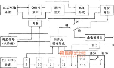
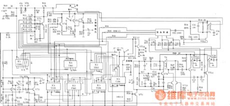
NTSC system signal generator is used in detecting and repairing multi-system color TV, satellite TV receiver, disc player, recorder, transistor and CD-G. The text is to introduce a practical, new, simple and cheap N system signal generator, whose field frequencies of 50Hz and 60Hz are changeable, apart from N system color stripes, octal stepped grey and grid, it can also generate a 50 travelling and 625 field checker grid. As the travel and field reference frequency is got by digital circuit frequency splitting, so the signal is stable and reliable, which can be the qualitative analysis detector.
(View)
View full Circuit Diagram | Comments | Reading(661)
Photoelectric control electric tracking toy vehicle circuit diagram
Published:2011/6/24 3:01:00 Author:Nicole | Keyword: photoelectric control, electric tracking toy vehicle

After 555 is triggered, in the period of temporary stability time, the high level which is outputed by 3 foot provides IC2 with work voltage. IC2 adopts analogue integrated circuit KD-5602, it contains didida general title sound, the music is about 10s. Once this chip obtains electricity and triggers, the general title sound will be performed, it is amplified by VT2, it drives loudspeaker to phonate. The typical work voltage of KD-5602 is +3V, so R4, DW steady voltage circuit are connected into circuit, 2CW51 provides +3V voltage. KD-5602's static power is tiny(Iab<1μA), the peripheral devices are few. R5, C5 are chip oscillator's external resistor capacitor components, the oscillation frequency or tone can be changed by adjusting RC time constant.
(View)
View full Circuit Diagram | Comments | Reading(540)
The audio signal generator of HFC5203A
Published:2011/6/26 5:31:00 Author:Borg | Keyword: audio signal, generator

In the figure is the audio signal generator, which can be used to detect radios, loudspeakers and other repairing instruments, and it characterizes little size, light weight, low power, simple structure, easy carry, and it's different from other signal generators that can only launch single frequency, it can output the continuous and repeated audio signals that are stored in the circuit storage. (View)
View full Circuit Diagram | Comments | Reading(803)
The precise nA stage current generator
Published:2011/6/26 20:55:00 Author:Borg | Keyword: precise, nA stage, current generator
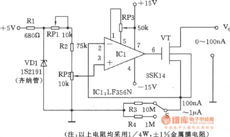
In real application, some special test circuits need the nA stage precise current as the reference, which is hard to make in the non-professional condition. In the figure is the precise nA stage current generator. This circuit is a constant micro current source. To make the current to be changed continuously and casually, as it is fixed with the multi-turn(10 turns) potentiometer as the divider to divide the reference voltage, so the value can be read out directly. Then by the current gear changing resistors of R3 and R4, the micro current of wide range is generated. (View)
View full Circuit Diagram | Comments | Reading(1409)
The headphone amplifier circuit (triode + op-amp opa2134)
Published:2011/6/26 20:59:00 Author:Borg | Keyword: headphone amplifier, op-amp
View full Circuit Diagram | Comments | Reading(3106)
Simple seconds pulse generator (CD4017)
Published:2011/6/20 8:29:00 Author:Lucas | Keyword: Simple , seconds, pulse generator
View full Circuit Diagram | Comments | Reading(2368)
Body induction music fountain switch circuit diagram
Published:2011/6/24 3:32:00 Author:Nicole | Keyword: body induction, music, fountain switch

The circuit is composed of inductive switch, monostable delay, music circuit and relay control circuit, the figure is as shown.
A inductive switch is made of metal sensor chip M and FET VT1(3DJ6). When somebody closes M chip, VT1's drain-to-source resistance increases, IC1's 2 foot level drops(≤1/3 VDD), 555 is set and it is high level, relay K pulls in, the contact turns from off to closed, the electric motor of water pump's power supply is connected, the fountain starts to spray water. At the same time, the music integrated circuit is triggered, and it sends out euphonious music. A monostable trigger circuit consists of 555 and R3, C2, the temporary stability duration time is td=1.1R3C3.
(View)
View full Circuit Diagram | Comments | Reading(1225)
| Pages:1692/2234 At 2016811682168316841685168616871688168916901691169216931694169516961697169816991700Under 20 |
Circuit Categories
power supply circuit
Amplifier Circuit
Basic Circuit
LED and Light Circuit
Sensor Circuit
Signal Processing
Electrical Equipment Circuit
Control Circuit
Remote Control Circuit
A/D-D/A Converter Circuit
Audio Circuit
Measuring and Test Circuit
Communication Circuit
Computer-Related Circuit
555 Circuit
Automotive Circuit
Repairing Circuit
