
Circuit Diagram
Index 1687
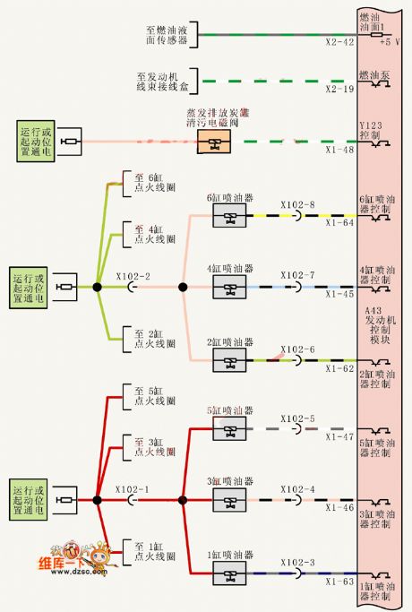
Shanghai Buick Royaum V63.6L car fuel system control circuit diagram(3)
Published:2011/6/24 4:24:00 Author:Nicole | Keyword: Shanghai Buick Royaum, car, fuel system control
View full Circuit Diagram | Comments | Reading(357)
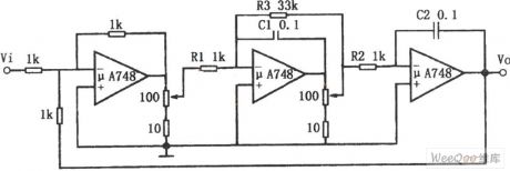
Multistage communication filter circuit
Published:2011/6/23 21:48:00 Author:TaoXi | Keyword: Multistage, communication, filter circuit
The filter circuit is as shown in the figure, the center frequency fc=1.180Hz, the gain Kv=1,C2=C3=C5=C6=C8.
(View)
View full Circuit Diagram | Comments | Reading(447)
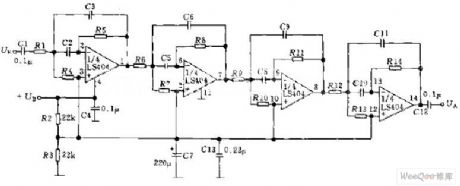
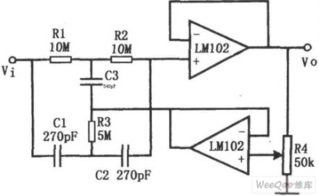
Active dual two-stage bandpass filter circuit
Published:2011/6/23 21:51:00 Author:TaoXi | Keyword: Active, dual, two-stage, bandpass filter
The active dual two-stage bandpass filter circuit is as shown in the figure, the center frequency is 1kHz, the quality factor Q=50, the gain Kv=100 (equivalent to 40 dB).
(View)
View full Circuit Diagram | Comments | Reading(754)
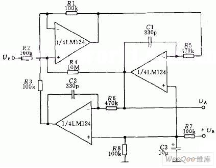
Frequency adjustable bandpass filter circuit
Published:2011/6/23 22:05:00 Author:TaoXi | Keyword: Frequency adjustable, bandpass, filter
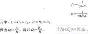
The frequency adjustable bandpass filter circuit is as shown in the figure. This filter's resonance frequency can be adjusted through the coaxial potentiometer, and the Q value will not change when you are adjusting the frequency. The Q value of the active band-pass filter of the figure is about 30, the resonant frequency can be changed from 150Hz to 1.5kHz, in this range the changing range of Q is less than 5%. For ease of the calculation, you need to set the potentiometer to the top, the resonant frequency f0 and the bandwidth B are:
Changing the position of the potentiometer is equivalent to add a voltage divider, so the current of R1, R2 and R3 reduce.
(View)
View full Circuit Diagram | Comments | Reading(2021)
High Q value trapped wave filter circuit
Published:2011/6/23 22:19:00 Author:TaoXi | Keyword: High Q value, trapped wave, filter circuit
The high Q value trapped wave filter circuit is as shown in the figure. Because the double-T network filter can have the better attenuation characteristics only when it is far away from the resonance frequency f0, so the Q value of the filter is not high. If the output signal of the filter is output by the voltage output device (the gain is 1), and it is feedback to the double-T network to form the bootstrap, so when the input signal attenuates for 0.3, the Q value is more than 50. The voltage follower is composed of the op-amp, the potentiometer R4 can continuously change the Q value of the circuit (from 0.3 to 50), the trapped wave frequency f0=1/2πR1C1.
(View)
View full Circuit Diagram | Comments | Reading(580)
DC voltage stabilization power supply LC filter circuit
Published:2011/6/23 21:54:00 Author:TaoXi | Keyword: DC, voltage stabilization, power supply, LC, filter circuit
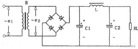
DC voltage stabilization power supply LC filter circuit (View)
View full Circuit Diagram | Comments | Reading(4049)
Narrow-band filter circuit with the adjustable Q value and frequency
Published:2011/6/23 22:28:00 Author:TaoXi | Keyword: Narrow-band, filter circuit, adjustable, Q value, frequency
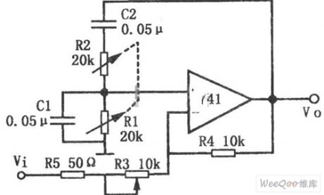
The narrow-band filter circuit with the adjustable Q value and frequency is as shown in the figure. This circuit is an active narrowband filter with adjustable Q value and frequency. It uses the Venturi bridge positive feedback, the loop gain is lower than 1. The feature of this circuit is if you adjust the Q value, you will not influence the center frequency. Because the Q value only has relationship with the gain of the return circuit. When the gain is 600, the Q value is 2000; when the gain is 140, the Q value is 30. In general venturi bridge oscillators, for the in-phase input ports, the amplifier gain must be more than 3 to start oscillation, the amplifier gain is less than 3 in this circuit.
(View)
View full Circuit Diagram | Comments | Reading(840)
Shanghai Buick Royaum V63.6L car air flow and inlet temperature sensor circuit diagram
Published:2011/6/24 4:27:00 Author:Nicole | Keyword: Shanghai Buick Royaum, car, air flow, inlet temperature sensor
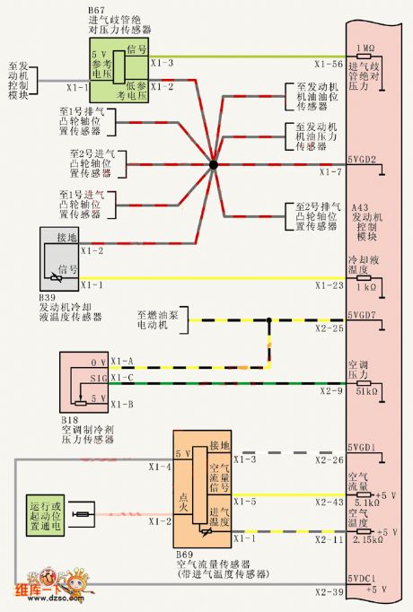
View full Circuit Diagram | Comments | Reading(366)
44V AC driving circuit
Published:2011/6/20 6:33:00 Author:TaoXi | Keyword: 44V, AC, driving circuit

The 44V AC driving circuit uses two power operational amplifiers 791, the continuous power consumption rated value of every power operational amplifier is 10W, and the amplifiers are connected into the AC electric bridge. The upper 791's reversed phase gain is 10, the lower 791's reversed phase gain is on the AC servo motor.
(View)
View full Circuit Diagram | Comments | Reading(594)
Trapped wave filter circuit uses the operational amplifier as the voltage follower
Published:2011/6/23 22:34:00 Author:TaoXi | Keyword: Trapped wave, filter circuit, operational amplifier, voltage follower
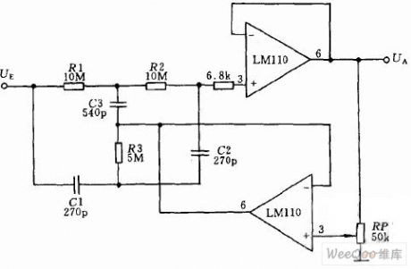
The trapped wave filter circuit which uses the operational amplifier (composed of two LM110 or SN72310) as the voltage follower is as shown in the figure.
(View)
View full Circuit Diagram | Comments | Reading(494)
555 long delay timer circuit 1
Published:2011/6/20 8:02:00 Author:TaoXi | Keyword: 555, long delay, timer circuit

This circuit is composed of the multivibrator (which is composed of the 555) and the monostable circuit. The oscillation frequency of the multivibrator f=1.44/(R1+R2+Rw)C1. The oscillation frequency of the figure parameters is about 600Hz. When the power turns on, the voltage of C5 can not change, so the set port has the low electrical level, the output port pin-3 has the high electrical level, the relay closes, the J1 closes to maintain the power supply; the J2 closes, the load operates. At this time, the internal disrharge tube which is connected with the pin-7 of the IC2 cuts off, the C3 is charged by the output of IC1 with the square-wave step type. When the threshold level is 2UDD/3, pin-3 has the low level, the timing time is up, the relay releases, the J1 and J2 cuts off, the load stops working.
(View)
View full Circuit Diagram | Comments | Reading(1069)
Infrared ray induction switch circuit
Published:2011/6/24 0:47:00 Author:TaoXi | Keyword: Infrared ray, induction switch

The infrared ray induction switch circuit that can be used in the infrared automatic hand washing device and the sit implement is as shown in the figure.
(View)
View full Circuit Diagram | Comments | Reading(630)
Simple flashing light circuit with the thyristor
Published:2011/6/24 0:52:00 Author:TaoXi | Keyword: Simple, flashing light, thyristor
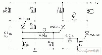
The MPU131 is designed as one kind of program-controlled thyristor that can be used in the relaxation oscillator circuit which is composed of the R1 and C1, the output of it respectively controls two unidirectional thyristors 2N5060 to make the low voltage (2V) indicator light to send out the timing flash.
(View)
View full Circuit Diagram | Comments | Reading(943)
FM transmitter over-voltage protection circuit
Published:2011/6/24 1:08:00 Author:TaoXi | Keyword: FM transmitter, over-voltage, protection circuit

The actuator of the FM302E—I FM transmitter uses the HPB-1210 motherboard which is produced by the NEC company. This device modulates the frequency of carrier wave directly, and it uses the phase-locked frequency stability technology and the frequency synthesis technology. The former stage power amplifier (BLF-177 mosfet) is directly promoted by the actuator, the maximum output power is 150W. The power adds to the final stage through the circulator that can be used as the driver stage of the last stage vacuum tube's power amplifier. The pre-amplifier power supply uses the 4NICK48 integrated power supply. Unfortunately, this stage has no over-voltage protection circuit and the DC voltage indication function, this makes this stage occurs some faults such as: the actuator output is normal, but this stage and the last stage have no output power.
(View)
View full Circuit Diagram | Comments | Reading(544)
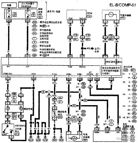
Shanghai Buick Royaum V63.6L car dynamical system interface module circuit diagram
Published:2011/6/24 4:30:00 Author:Nicole | Keyword: Shanghai Buick Royaum, car, dynamical system, interface module
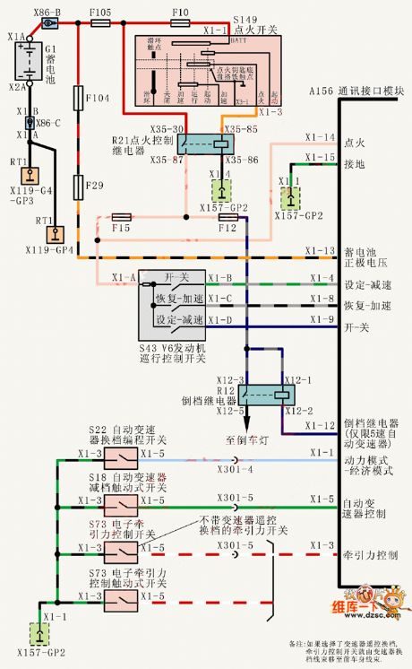
View full Circuit Diagram | Comments | Reading(386)
Meishun ME-308 pure DC current negative feedback class A power amplifier circuit
Published:2011/6/18 10:18:00 Author:Nancy | Keyword: pure DC current, negative feedback, power amplifier, class A

View full Circuit Diagram | Comments | Reading(1771)
Motor phase broken phase protector circuit
Published:2011/6/24 1:28:00 Author:TaoXi | Keyword: Motor phase, broken phase, protector circuit
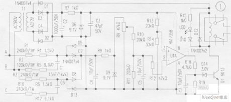
Working principle:
The A, B, C are connected with the A, B, C phases of the AC380V power line network, the phase-shift circuit is composed of the R1, R4, R2, R5, C1, R3, R6, R16, R17, C6. When the voltage is normal (the phase sequence is correct and no phase-lack), the vector voltage of the rectifier input port which is composed of the diodes D5, D7, D8, D13 is small, the rectified voltage is small too. When the phase sequence is wrong or the phase is incomplete, the output voltage instantaneous up to 13V. The voltage is filted by V4, limited by R8 and then is stabilized by D9, at last it is send to the pin-2 of the comparator LM358 through the current limiting resistor R12, it is used as the detected signal voltage.
(View)
View full Circuit Diagram | Comments | Reading(1059)
Nissan A32-EL board computer circuit
Published:2011/6/22 10:19:00 Author:Nancy | Keyword: Nissan, board computer
View full Circuit Diagram | Comments | Reading(495)
Nissan A32-EL warning lamp circuit 2
Published:2011/6/22 10:21:00 Author:Nancy | Keyword: Nissan, warning lamp
View full Circuit Diagram | Comments | Reading(377)
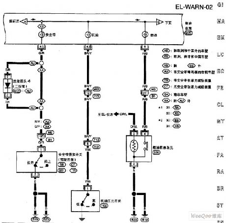
Nissan A32-EL warning lamp circuit 4
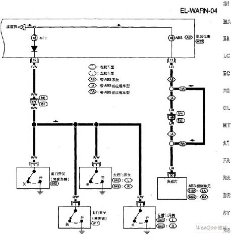
Published:2011/6/22 10:23:00 Author:Nancy | Keyword: Nissan, warning lamp
View full Circuit Diagram | Comments | Reading(370)
| Pages:1687/2234 At 2016811682168316841685168616871688168916901691169216931694169516961697169816991700Under 20 |
Circuit Categories
power supply circuit
Amplifier Circuit
Basic Circuit
LED and Light Circuit
Sensor Circuit
Signal Processing
Electrical Equipment Circuit
Control Circuit
Remote Control Circuit
A/D-D/A Converter Circuit
Audio Circuit
Measuring and Test Circuit
Communication Circuit
Computer-Related Circuit
555 Circuit
Automotive Circuit
Repairing Circuit