
Circuit Diagram
Index 1691
Hitting target sphere "wishing you prosperity" pronunciation alarm circuit diagram
Published:2011/6/23 22:40:00 Author:Nicole | Keyword: target sphere, wishing you prosperity, pronunciation alarm
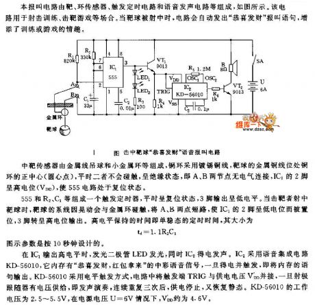
The hitting target sensor is composed of gold line drop ball and small gold loop, the copper loop adopts tinned copper wire, the target ball's gold copper wire is in the midpoint(center point)of copper ring, ordinarily, they will not touch, they are in insulation state, namely, the two points of A, B have no electricity connection, IC1's 2 foot is high level(VDD), the 555 circuit is in reset state.
A trigger timer is made of 555 and R2, C1, ordinarily, it is in reset state, 3 foot output is low level. When people hit the target, the tie line of target will touch the gold loop due to shake, then A, B points are short circuit, IC1's 2 foot is low level and it is set, 3 foot turns to high level output. The high level's hold time, namely, the monostable timing time is td=1.1R2C1.
(View)
View full Circuit Diagram | Comments | Reading(462)
The simple square wave generating circuit of TL082
Published:2011/6/14 3:32:00 Author:Borg | Keyword: square wave, generating circuit

This circuit is a rectangular and square circuit, the time of the high/low LEV can be set separately, the oscillating frequency is decided by high and low LEV time. In the circuit, the resistors which decide the charging/discharging time of capacitor C are shifted by diodes, and the square wave high/low LEV time can be regulated by changeable resistors R1 and R2. The resistance net RA is the feedback circuit and the charging/ discharging circuit of capacitor C for the op-amp. The output voltage of the op-amp is split by the resistors of 56kΩ and 47kΩ and becomes the reference voltage, it compares with the voltage on capacitor C and then generates the oscillation. (View)
View full Circuit Diagram | Comments | Reading(1581)
Motor control circuit with the transistor and the single thyristor
Published:2011/6/23 2:30:00 Author:TaoXi | Keyword: Motor, control circuit, transistor, single thyristor

This circuit uses the transistor phase shifting trigger and the unidirectional thyristor to control the full wave voltage of the series excitation motor circuit, so we can control the motor speed in the wide range. The resistor R5 is connected in the unidirectional thyristor main circuit in series to form the negative feedback, this method can steady the speed. The numerical value of R5 is 0.1~1Ω. The function of the diode rectifier bridge Br is to change the AC into DC.
(View)
View full Circuit Diagram | Comments | Reading(505)
The precise gated oscillator
Published:2011/6/13 20:19:00 Author:Borg | Keyword: precise, gated oscillator
Many gated oscillator circuit generates wave of which the first period tends to be too long or too short, and not stable, too. In the figure is a gated oscillator which is made of a dual-trigger circuit 74SL221, whose wave is stable and pure, and its edge is delivered from one stage to the next stage, so it is precise. The two triggers have the same functions, and their oscillating frequencies are about l/1.4R1·Cl and 1/1.4R2·C2, the maximum value of the actual frequency is 10MHz. The wave outline circuit is as follows:
(View)
View full Circuit Diagram | Comments | Reading(535)
Serving guest doorbell and dog alarming circuit diagram
Published:2011/6/23 22:11:00 Author:Nicole | Keyword: Serving guest doorbell, dog alarming

The monostable trigger circuit is composed of IC2-m(1/2 556)and R3, C3, its monostable working time is decided by R3, C3's charge time constant, the monostable time is t1=1.1R3C3. The graphic parameter t1 is about 100s. In the period of IC2-a is set, VT3 is saturation conduction, VT4 cut off, C5 changes from the short circuit state to charge state. The delay control circuit is made of IC2-b(1/2 566)and R5, C5, the delay depends on the R5C5's charge time constant, namely, when IC1-b(1/2 566)'s 8 foot and 12 foot are dropped to 1/3VDD by C5's charge, 1/2 566 is set, 9 foot turns to high level, then the dog braying analog integrated circuit(HFC5201)obtains electricity and it sends out barking. The barking time t2 is t2=1.1R5C5. The graphic parameter t2 is about 1 minute.
(View)
View full Circuit Diagram | Comments | Reading(613)
Charge pump circuit
Published:2011/6/23 2:42:00 Author:TaoXi | Keyword: Charge pump

The charge pump phase locked loop has the features of low power consumption, high speed, little jitter and low cost, it can be used in the wireless communication, the frequency synthesizer and the clock recovery circuit. The charge pump circuit plays the very important role in the phase locked loop(PLL), the main function of it is to change the UP and DOWN digital signals of the PFD into the analog signal, so we can control the frequency of the voltage-controlled oscillator (VCO). When the PFD gives the high precision phase error, the charge pump plays a decisive role to the performance of the whole loop.
(View)
View full Circuit Diagram | Comments | Reading(785)
Voltage Control Function Generator Circuit of μA709
Published:2011/6/25 21:45:00 Author:Michel | Keyword: Voltage Control, Function Generator, Circuit

The picture 6-50 is the voltage control function generator circuit of μA709.In the circuit,A1 is charge reversal circuit,VT1~VT4 are analog switches,A2 is mueller integral circui,A3 and A4 are PWL comparing circuit,VT6,VT5 and G1-G3 are trigger circuit.VT1 and VT2 analog switches control voltgae UT to control the operational amplifier A1, integrating circuit's intergration composed of timing resistance RT (RT1 and RT2) and the forms of A2 output linear rising and fall.If VT1 conducts,A2 output linear declines because positive step voltgae intergrates. (View)
View full Circuit Diagram | Comments | Reading(2034)
The auto VGA synchronized signal generator
Published:2011/6/13 20:38:00 Author:Borg | Keyword: synchronized signal generator
See as the figure, no matter what polarity of the input signal is, the circuit can generate a passive synchronized pulse. The 5v voltage which is imposed on R1 and R2 is split into two 2.5V voltages, so that we don't needed to magnify the input signal. The RC net of R3C1, which is on a OR gate terminal, can keep 2-pin in a high LEV when there is an external passive synchronized pulse, because the passive synchronized pulse is very narrow, which makes the capacitor C2 charges under the limited voltage; therefore, the pulse is no inverted. The a positive pulse is input, the LEV of 2-pin is not allowed to be raised, so the input is inverted. (View)
View full Circuit Diagram | Comments | Reading(529)
Micro vibration sensor alarming circuit diagram
Published:2011/6/23 21:51:00 Author:Nicole | Keyword: Micro vibration, sensor alarming
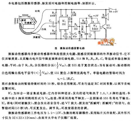
This circuit includes micro vibration sensor, trigger delay circuit and control circuit, the figure is as shown.
The micro vibration sensor contains vibration sensor device and high power amplifier circuit, it can induce very weak external vibration signal, it has high sensitivity, and its output voltage signal can push the backward stage circuit directly. The monostable trigger cirucit consists of 555 and R1, R2, R3, C3, ordinarily, due to the partial pressure(1/2VDD)of R1, R2 voltage dividers, 555 is in reset state; when it is vibration, the vibrator's white line outputs low level signal(<1/3VDD), 555 is set, 3 foot turns to high level. The short steady time of the monostable circuit is td=1.1R3C3. The short steady duration time of graphic parameter is about 50s.
(View)
View full Circuit Diagram | Comments | Reading(2376)
The sine and square wave generator (ICL8038、SN7473、MC1445L)
Published:2011/6/14 1:34:00 Author:Borg | Keyword: wave generator

Generally, when measuring the dynamic range and distortion of the linear amplifier, we need the sine wave; when measuring the transient state, frequency character and phase distortion, we need the square wave. This circuit has three working states, i.e sine wave output, square wave output or the auto-changed sine/square wave output. In the figure, ICL8038 is a multi-wave generator, whose output sine waves and square waves are imposed on the two poles of the video amplifier MC1445l. The square waves, which are outputed by the generator, are imposed on the counting pole of the TTL four point frequency circuit (SN7473). (View)
View full Circuit Diagram | Comments | Reading(2428)
Oscillation and impact acousto-optic alarm circuit diagram
Published:2011/6/23 21:25:00 Author:Nicole | Keyword: Oscillation, impact, acousto-optic alarm

The sensor is composed of tinned gold ball which is hung on gold spring wire and small gold box, the ball is hung on the center of the box, it has 1~2mm gap, it can not be touched in the condition of state, namely, the electricity is isolated, the ball is connected to power supply VDD, the box is connected to R1 and VT1. When it has impact or oscillation, the ball will thrill or shake, and it is connected to the gold, VT1 obtains positive bias and turns on. Due to C2 charging capacitor is connected, even slight impact or oscillation, VT1 also can keep constant turn-on, then IC1, IC2 will obtain ground loop, VT1's saturated voltage drop is not higher than 0.4V.
IC1 adopts time base circuit 555, the low frequency multivibrator is made of IC1 and R2, R3, R4, the oscillation frequency is fc=1.44/(R2+2R3)C3.
(View)
View full Circuit Diagram | Comments | Reading(1655)
Low voltage band gap reference circuit
Published:2011/6/23 2:48:00 Author:TaoXi | Keyword: Low voltage, band gap, reference circuit

In order to meet the low voltage application of the band gap reference circuit, we use the current mode structure low voltage band gap reference circuit which is as shown in the figure. This circuit can output the voltage that is lower than 1V, this effectively reduces the power supply voltage of the circuit, at the same time this circuit uses the two-stage op amp with the negative feedback network and the Bias which has no relationship with the voltage to reduce the power sensitivity of the circuit.
(View)
View full Circuit Diagram | Comments | Reading(2473)
The sawtooth wave generating circuit of 555
Published:2011/6/14 0:13:00 Author:Borg | Keyword: sawtooth wave


In the figure is the sawtooth wave generating circuit of 555. The circuit is a audio sawtooth wave generator which is irrelevant to temperature, whose linearity is within 1%. It uses the timer NE555 to make a non-steady multi-oscillator. The capacitor C1 is charged by the power supply(+5V) with the help of R1,R2 and R3, and discharge is done through R3 and the transistor channel inside NE555, therefore, the sawtooth wave is generated on 7-pin of NE555. The wave is output by the emitter Q1(MPS-AB) of the Darlington transistor. The output of Q1 is reacted to the upper part of R2 by C2.
(View)
View full Circuit Diagram | Comments | Reading(1014)
The simple frequency multiplication generator
Published:2011/6/13 20:51:00 Author:Borg | Keyword: frequency multiplication generator
In the figure is the frequency multiplication circuit which consists of OR gates, the stepping-down edge of the input signal is differentiated by R1C1 and sent to the input terminal(3-pin) of A2, which makes A2 output a pulse, the stepping-up edge A1 is inverted and then it is sent to the input terminal(4-pin) of A2, so that A2 outputs a pulse again. As a result, by inputting a square wave, we can get two square waves at the output terminal of A2, and the frequency is doubled. A3 functions as the buffer and the rectifier. The wave outlines of the input signal are shown in the following figure.
(View)
View full Circuit Diagram | Comments | Reading(650)
The simple triangular and square wave generating circuit composed of TL082
Published:2011/6/15 21:47:00 Author:Borg | Keyword: square wave, generating circuit
In the figure is the simple triangular and square wave generating circuit composed of TL082. This circuit consists of the integrator, which is composed of computing amplifier, and the lag comparator circuit. In the figure, R1 and C form a integrating time constant, which is used to change the oscillating frequency. R2 can not only change the amplitude of the triangular wave, but also change its frequency. Besides, the oscillating frequency is effected by the output voltage of the lag comparator. Whether the output LEV is high or not is decided by the op-amp saturation and voltage. Due to the discreteness of the elements, the symmetry of the waveform is effected. (View)
View full Circuit Diagram | Comments | Reading(2946)
The ultra-low frequency triangular wave generating circuit (747、μA723)
Published:2011/6/14 0:37:00 Author:Borg | Keyword: ultra-low frequency, triangular wave
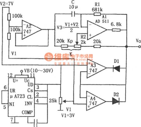
The circuit is an ultra-low frequency oscillator consisting of precise clamper circuit, which is almost a standard non-steady multi-resonance oscillator. In the figure, A3 and A4 form a symmetric precise clamper amplitude-limited circuit, with the clamper technology, the expensive voltage steady diode of temperature compensation is not needed, the feature of the circuit is that the stabilization depends only on the stabilization of the power supply voltage, and just the single polarity voltage can fulfill the dual polarity clamping. The reference voltages V1 and V2 on A3 and A4 are supplied by the reference voltage source μA723. (View)
View full Circuit Diagram | Comments | Reading(700)
The receiving party modem and single-chip microcomputer interface circuit
Published:2011/6/23 21:14:00 Author:TaoXi

The receiving party modem circuit and the battlefield sensor modem circuit have the same using and control methods in the single-chip microcomputer and the demodulation chip. The different is the second serial port of the single-chip microcomputer is connected with the RS 232C port of the computer through the level conversion circuit, it sends the received digital signal to the PC. The receiving party modem and single-chip microcomputer interface circuit is as shown in the figure. The D1~D8 are the receive data display, the D9 is the system power indicator, the D10 is the correct sending indicator, the D11 is the carrier wave detection indicator, the D12 is the data transmission indicator.
(View)
View full Circuit Diagram | Comments | Reading(483)
The pulse frequency doubler composed of gate circuits (CD4011)
Published:2011/6/17 6:33:00 Author:Borg | Keyword: pulse frequency doubler, gate circuits
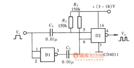
The pulse frequency doubler consists of two gates of the NAND CD4011, and one of the gates forms the phase inverter. By inputting the falling edge inverting phase of the pulse, the circuit will output a pulse with the help of the rising edge and the falling edge of the pulse, so that the aim of double frequency is fulfilled. The circuit construction is as follows.
(View)
View full Circuit Diagram | Comments | Reading(4213)
The AD108 frequency doubler allowing asymmetric square wave input
Published:2011/6/17 8:23:00 Author:Borg | Keyword: frequency doubler, asymmetric square wave
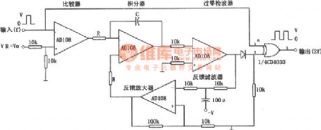
In the figure is the frequency doubler allowing asymmetric square wave input. This circuit characterizes wide frequency range, and it is not affected by the power supply voltage change, it also receives asymmetric input signals. When the input is a square wave, the input signal is turned into a dual polarity wave by a high gain comparator and then added on an integrator. The input of the integrator is the triangular wave. The wave crosses the zero line at T/4 and 3T/4(T is the period of the input signal), after the triangular wave has been sent to the zero detector, the 90⁰ lagged phase square wave is generated. (View)
View full Circuit Diagram | Comments | Reading(1129)
Bandwidth adjustable audio filter circuit with the 900Hz center frequency
Published:2011/6/23 21:19:00 Author:TaoXi | Keyword: Bandwidth, adjustable, audio filter, 900Hz, center frequency

This circuit uses the Wien-bridge, it has the adjustable bandwidth and the center frequency is 900Hz, if the 10K potentiometer's level is too low, there will be the circuit oscillation.
(View)
View full Circuit Diagram | Comments | Reading(775)
| Pages:1691/2234 At 2016811682168316841685168616871688168916901691169216931694169516961697169816991700Under 20 |
Circuit Categories
power supply circuit
Amplifier Circuit
Basic Circuit
LED and Light Circuit
Sensor Circuit
Signal Processing
Electrical Equipment Circuit
Control Circuit
Remote Control Circuit
A/D-D/A Converter Circuit
Audio Circuit
Measuring and Test Circuit
Communication Circuit
Computer-Related Circuit
555 Circuit
Automotive Circuit
Repairing Circuit