
Circuit Diagram
Index 1701
The high stability pulse period gradual spread circuit
Published:2011/6/25 21:19:00 Author:qqtang | Keyword: high stability, pulse period

In the figure is the high stability pulse period gradual spread circuit. In the circuit, NE555(1) compose the pulse gradual spread timing circuit, NE555(2) compose the single steady trigger circuit, the NE555(1) and NE555(2) are connected by VD1. Before the key is pressed, the transistor inside NE555(2) is conducting, its 3-pin is outputting a low LEV, the diode VD1 is conducting and the voltage on capacitor C1 is 0, so the NE555(1) timer can't work.
When S1 is pressed, it will shake for some time. (View)
View full Circuit Diagram | Comments | Reading(1111)
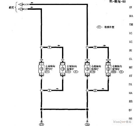
Nissan A32-EL warning lamp circuit 3
Published:2011/6/22 10:22:00 Author:Nancy | Keyword: Nissan, warning lamp
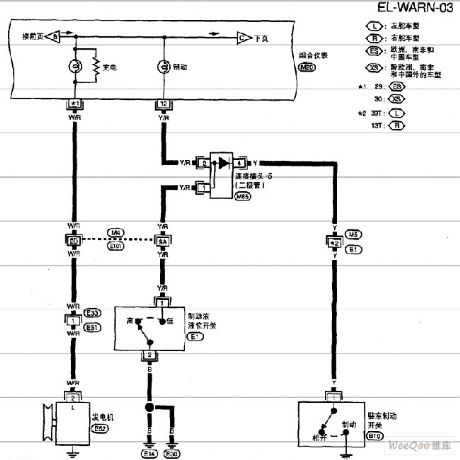
View full Circuit Diagram | Comments | Reading(495)
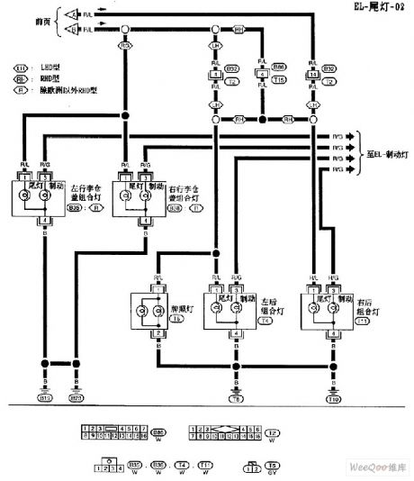
Nissan A32-EL front fog lamp circuit 2
Published:2011/6/22 9:59:00 Author:Nancy | Keyword: Nissan, front fog lamp
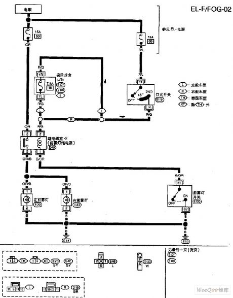
View full Circuit Diagram | Comments | Reading(449)
Nissan A32-EL front fog lamp circuit 1
Published:2011/6/22 9:57:00 Author:Nancy | Keyword: Nissan, front fog lamp
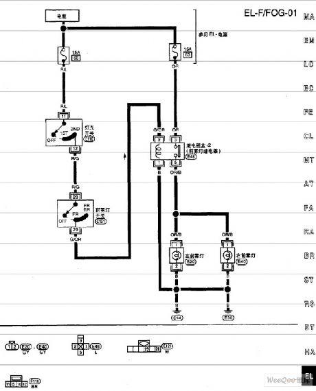
View full Circuit Diagram | Comments | Reading(418)
Teana A33-EL indoor lamp 3
Published:2011/6/22 9:55:00 Author:Nancy | Keyword: Teana, indoor lamp

View full Circuit Diagram | Comments | Reading(499)
Teana A33-EL indoor lamp 2
Published:2011/6/22 9:54:00 Author:Nancy | Keyword: Teana, indoor lamp

View full Circuit Diagram | Comments | Reading(486)
Teana A33-EL indoor lamp 1
Published:2011/6/22 9:52:00 Author:Nancy | Keyword: Teana, indoor lamp

View full Circuit Diagram | Comments | Reading(455)
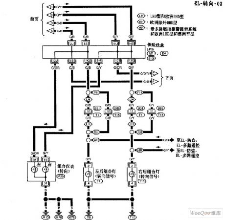
Nissan A32-EL lighting circuit 1
Published:2011/6/22 9:01:00 Author:Nancy | Keyword: Nissan, lighting circuit
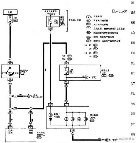
View full Circuit Diagram | Comments | Reading(379)
The protection circuit of IBA base power supply system
Published:2011/6/20 9:56:00 Author:Nancy | Keyword: IBA base power supply system, protection circuit
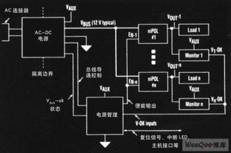
In many computer and communication applications, non-isolation load point (niPOL) Intermediate Bus Architecture (IBA) converter is replacing continuously the common distribution and central power supply system. The key drive force of the trend includes: the increase of the system power, higher output current, more strict regulated requirements and lower system cost, many IBA/niPOL solutions can meet these requirements. However,this solution don't have the protection mechanism included in the previous common solutions. In the power supply system design, over-voltage protection (OVP) and over-temperature protection is very expectable. (View)
View full Circuit Diagram | Comments | Reading(470)
The wireless reception headphone circuit
Published:2011/6/24 21:57:00 Author:qqtang | Keyword: wireless, reception, headphone

TDA2822-B-B wireless reception headphone is the tool that students receive the teaching audio. The writer has drawn a physical map, which is shown in the figure as reference.
See as the figure, TDA2822M is the dual-channel audio amplifier integrated circuit (in the figure there is one channel). The magnet coil S receives the audio signal from the audio classroom, the signal is sent to the 6-pin of the chip by the central head of potentiometer W, and then it is amplified and output by 3-pin, finally, it passes the coupling capacitor C2 and is added on the headphones in parallel connection, so the headphone is making sounds. (View)
View full Circuit Diagram | Comments | Reading(931)
The regulated circuit composed of LM317
Published:2011/6/24 21:45:00 Author:qqtang | Keyword: regulated circuit

View full Circuit Diagram | Comments | Reading(718)
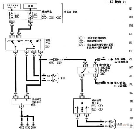
Nissan A32-EL embarkation lamp circuit 5
Published:2011/6/20 9:39:00 Author:Nancy | Keyword: Nissan, embarkation lamp
View full Circuit Diagram | Comments | Reading(395)
The timing circuit composed of the 555(ICM7555)of CMOS
Published:2011/6/25 21:32:00 Author:qqtang | Keyword: timing circuit, 555

In the figure is the timing circuit composed of the 555(ICM7555)of CMOS, as CMOS is used, the impedance is very high, therefore, the amplitude of the time can be expanded largely, for example, it can compose a timer of several minutes. Here, figure (a) is the simple timing circuit.
In Figure (b) is a timing circuit which can set the time of 10~100s, in the circuit, to use to differential pulse trigger, the capacitor C1 is used for coupling, only when the voltage of 2-pin is lower than 1/3 of the power supply is the trigger motivated. The time is decided by C3 and R4+RP1. (View)
View full Circuit Diagram | Comments | Reading(1319)
Nissan A32-EL embarkation lamp circuit 4
Published:2011/6/20 9:38:00 Author:Nancy | Keyword: Nissan, embarkation lamp
View full Circuit Diagram | Comments | Reading(391)
20W OCL power amplifier circuit
Published:2011/6/13 8:31:00 Author:Christina | Keyword: 20W, OCL, power amplifier

The circuit is as shown in the figure. The feature of the OCL power amplifier: the speaker is directly coupled with the output port of the amplifier. The circuit uses the positive and negative symmetrical power supply and the differential amplifier as the input port that can guarantee the zero DC potential, so it has good fidelity. The VT1 and VT2 can use the S3DG6 differential geminating tube.
Figure The 20W OCL power amplifier circuit
(View)
View full Circuit Diagram | Comments | Reading(3748)
Nissan A32-EL embarkation lamp circuit 3
Published:2011/6/20 9:37:00 Author:Nancy | Keyword: Nissan, embarkation lamp
View full Circuit Diagram | Comments | Reading(413)
Nissan A32-EL embarkation lamp circuit 2
Published:2011/6/20 9:36:00 Author:Nancy | Keyword: Nissan, embarkation lamp
View full Circuit Diagram | Comments | Reading(410)
Radio intermediate frequency amplifier circuit
Published:2011/6/13 8:20:00 Author:Christina | Keyword: Radio, intermediate frequency, amplifier

The intermediate frequency amplifier circuit of the general semiconductor radio is as shown. The 465kHz intermediate frequency signal which is produced by the frequency changing circuit is sent to the VT2 by the secondary stage of the intermediate frequency transformer T2 to be amplified, the amplification signal is sent to VT3 by the T3 intermediate frequency transformer to be amplified again, then it is sent to the wave detector by the T4 intermediate frequency transformer to be detected, the detected signal is sent to the low frequency amplification stage to be amplified.
The CN is the neutralizing capacitance of the circuit that can be used to inhibit the intermediate frequency parasitic oscillation.
Figure The radio intermediate frequency amplifier circuit
(View)
View full Circuit Diagram | Comments | Reading(1733)
The 555 basic timing circuit
Published:2011/6/24 23:14:00 Author:qqtang | Keyword: basic timing

In the figure is the 555 basic timing circuit. In the circuit, if we add a figured trigger pulse on the 2-pin of 555, the 3-pin will output a intermittent pulse, the interval time is T≈RC. After being amplified by VT1, the signal drives the relevant circuit, such as the LED in the figure.
(View)
View full Circuit Diagram | Comments | Reading(500)
The long-span timing circuit
Published:2011/6/24 21:32:00 Author:qqtang | Keyword: long-span, timing
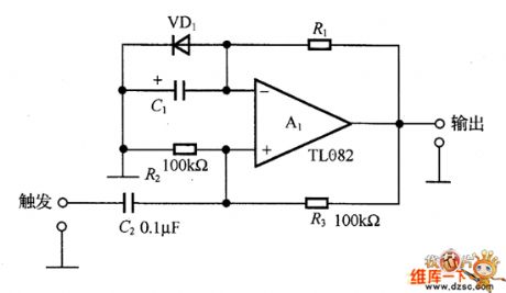
In the circuit is the long-span timing circuit. In the circuit, A1 is a FET input op-amp TL082, the voltage on the non-inverting is half of the saturating voltage(about 12V), and the voltage of the inverting terminal is fixed at +.0.6V due to the conduction of VD1. If the triggering terminal is input with a higher than 6V passive pulse, A1 is in passive saturation, at the moment, the non-inverting terminal is in a -6V voltage, the capacitor C1 is charging back with the help of R1, is the charging voltage is over -0.6, A1 output is in positive saturation, then a period is over. The charging time is T=R1C1ln(R2+R3)/R3.
(View)
View full Circuit Diagram | Comments | Reading(768)
| Pages:1701/2234 At 2017011702170317041705170617071708170917101711171217131714171517161717171817191720Under 20 |
Circuit Categories
power supply circuit
Amplifier Circuit
Basic Circuit
LED and Light Circuit
Sensor Circuit
Signal Processing
Electrical Equipment Circuit
Control Circuit
Remote Control Circuit
A/D-D/A Converter Circuit
Audio Circuit
Measuring and Test Circuit
Communication Circuit
Computer-Related Circuit
555 Circuit
Automotive Circuit
Repairing Circuit