
Circuit Diagram
Index 1705
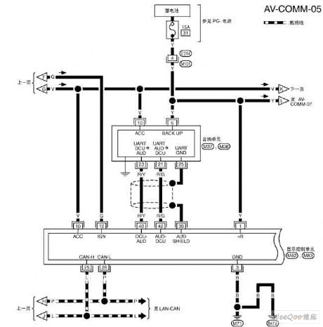
NISSAN new Teana navigation system circuit 14
Published:2011/6/18 21:23:00 Author:Nancy | Keyword: NISSAN, Teana navigation system
View full Circuit Diagram | Comments | Reading(623)
NISSAN new Teana navigation system circuit 13
Published:2011/6/18 21:22:00 Author:Nancy | Keyword: NISSAN, Teana navigation system
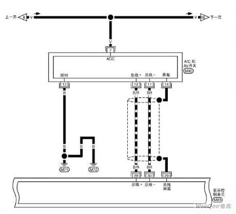
View full Circuit Diagram | Comments | Reading(659)
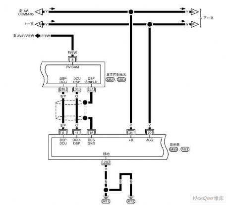
NISSAN new Teana navigation system circuit 12
Published:2011/6/18 21:21:00 Author:Nancy | Keyword: NISSAN, Teana navigation system
View full Circuit Diagram | Comments | Reading(615)
555 time relay circuit
Published:2011/6/20 8:46:00 Author:TaoXi | Keyword: 555, time relay

This circuit is composed of the +12V voltage stabilization circuit, the 555 monostable circuit and the relay control circuit, when the power is connected, pin-2 has the low level, the 555 sets, the relay J2 will not act, when the voltage of C2 is charged to 2VDD/3, the pin-3 has the low level, the J2 closes to connect the contact points J2-1 and J2-2. The NC contact point J1 of the relay J1 will cut off after the circuit got the power. This circuit can replace the JSJ1 transistor time relay. The timing parameters are as shown:
(View)
View full Circuit Diagram | Comments | Reading(529)
The defroster, warmer and air-conditioning system circuit of the Southeast Delica lightweight bus
Published:2011/6/25 22:05:00 Author:qqtang | Keyword: defroster, warmer, air-conditioning system, lightweight bus

The defroster, warmer and air-conditioning system circuit of the Southeast lightweight bus is shown as above.
Delica (View)
View full Circuit Diagram | Comments | Reading(1268)
555 approach switch circuit
Published:2011/6/20 8:35:00 Author:TaoXi | Keyword: 555, approach, switch circuit

The approach switch circuit is the monostable trigger which is composed of the 555. The trigger port pin-2 of 555 is connected with the power supply voltage port through the high value resistance, it is in the standby state. When the human body approaches or touches the metal plate, the induction signal 555 is triggered to output a monostable pulse. The C2 can be used in the anti-disturbance filtering. This circuit can be used in the electrical equipments, the toys and the alarm circuits.
(View)
View full Circuit Diagram | Comments | Reading(540)
The 24V regulated power supply of current limiting protection function
Published:2011/6/24 23:16:00 Author:qqtang | Keyword: regulated power supply, current limiting, protection

View full Circuit Diagram | Comments | Reading(671)
The dual-way converting switch typical circuit with lock
Published:2011/6/24 23:23:00 Author:qqtang | Keyword: dual-way, converting switch, typical circuit


In the figure is circuit of the dual forward trigger SN7474 with presetting and clearance, and the analog switch SW7510EQ. Its control encoding and switch stage are shown in the table.
(View)
View full Circuit Diagram | Comments | Reading(701)
The 0~20v regulated power supply circuit
Published:2011/6/24 23:29:00 Author:qqtang | Keyword: regulated power supply

View full Circuit Diagram | Comments | Reading(627)
BA5049 infrared remote control signal receiving integrated circuit
Published:2011/6/21 2:06:00 Author:Christina | Keyword: infrared, remote control, signal, receiving integrated circuit
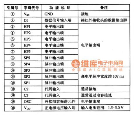
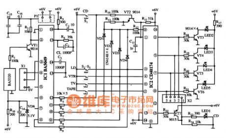
The BA5049 is designed as one kind of multi-channel infrared remote control signal receiving integrated circuit which is produced by the ROHM company, and it can be used in the infrared remote control system of the small home appliances such as the TianYi AD-51OOA power amplifier.
1.Features
The BA5049 is composed of the remote control signal preamplifier, the automatic level control circuit, the clock oscillating circuit, the pulse output circuit, the code signal processing circuit and other subsidiary function circuits.
2.Pin functions
The BA5049 is in the 16-pin dual-row DIP plastic package, the pin functions are as shown in table 1.
Table 1 The pin functions of the BA5049
3.Typical application circuit
The remote control signal receiving typical application circuit which is composed of the BA5049 is as shown in figure 1.
Figure 1 The typical application circuit of BA5049
(View)
View full Circuit Diagram | Comments | Reading(3063)
The door-lock system and affiliated electric circuit of the Southeast Delica lightweight bus
Published:2011/6/25 22:08:00 Author:qqtang | Keyword: door-lock system, affiliated electric circuit, lightweight bus
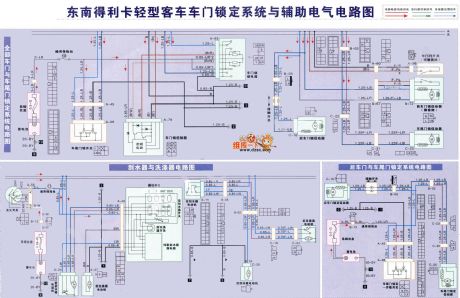
The door-lock system and affiliated electric circuit of the Southeast Delica lightweight bus is shown as above.
(View)
View full Circuit Diagram | Comments | Reading(1306)
25W continuous 28W peak value multi-output power supply circuit
Published:2011/6/19 18:58:00 Author:TaoXi | Keyword: 25W, continuous, 28W, peak value, multi-output, power supply

The power supply of the DVD or the set-top box in the figure is designed as the flyback converter with the TNY280PN(U1). In this design, the 10μF capacitance C4 uses the enhanced current-limit point of U1, this point makes the power supply to output the 28W peak power when the device is starting or in the load transient. The 25W continuous 28W peak value multi-output power supply is in every enable switching cycle, the MOSFET of the U1 conducts, the current gets through the primary winding of the transformer T1. When the primary stage current reaches the MOSFET current-limit point, the MOSFET turns off, the energy of the transformer T1 is transmited to the secondary stage. The over-voltage protection is realized by the U2, R12, R13, VR1 and VR2.
(View)
View full Circuit Diagram | Comments | Reading(2521)
BA38805 audio phase and harmonic distortion correction integrated circuit
Published:2011/6/22 7:27:00 Author:Christina | Keyword: audio phase, harmonic distortion, correction, integrated circuit

The BA3880S is one kind of audio phase and harmonic distortion correction integrated circuit that is produced by the ROHM company. It can be used in wide range of applications such as the domestic and imported sound systems, the TV sound systems and the computer audio systems.
1.Features
The BA38805 can compensate the distortion which is caused by the power amplifier and speaker characteristics to reproduce the original audio signal.
2.Pin functions and data
The BA38805 is composed of the left and right sound channels mixed amplifier, the left and right sound channels voltage control amplifier, the left and right sound channels peak level detector, the the left and right sound channels high-pass and low-pass filter, and the reference voltage circuit.
Table 1 The pin functions and data of the BA38805
(View)
View full Circuit Diagram | Comments | Reading(916)
The fast speed analog switch circuit
Published:2011/6/25 1:21:00 Author:qqtang | Keyword: fast speed, analog switch

The we need to fast, exactly and reliably change or put through the high LEV, we can use the figured circuit (such as the digital, synchronized converter). The feedback net can output stable signals, which can offset the effect caused by the output change of circuit parameters. The DC input signals in the range of ±10V and the -20V DC voltage on the FET transistor grid work together, which makes the input channel blocked. The input channel is put through when FET transistor grid is +10V, and then the grid is output by the op-amp.
(View)
View full Circuit Diagram | Comments | Reading(570)
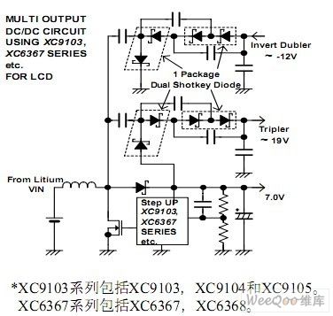
Charge pump multi-voltage output circuit composed of Walter Schottky diodes
Published:2011/6/19 10:36:00 Author:TaoXi | Keyword: Charge pump, multi-voltage, output circuit, Walter Schottky diodes
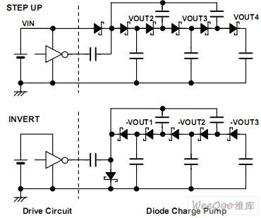
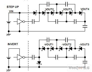
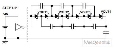
Circuit principle:
The basic circuit is as shown in figure 1.
The output voltage is as shown, the output voltage VOUT1, VOUT2, VOUT3 is the 1, 2, 3 times of the input voltage respectively. The rising voltage produces the N(>=2) times voltage by using the single power supply and the clock pulse; the reversal uses the clock pulse to produce the -N(>=1) times voltage.
Figure 2 is the changed circuit, the rising time of it is shorter than the basic circuit, but the stability is poor.
Figure 3 is the method which only uses the clock pulse to produce the rising voltage. Although you need to add some schottky diodes and capacitances in the circuit, but you do not need the single power supply.
Figure 4 is the multi-power application example which is composed of the figure 3 circuit. This design can be used in the PDA and LCD applications, because this device can produce multiple groups of positive and negative voltage output by using a single channel DC/DC converter, such as the 9103 series.
Figure 1 The basic circuit 1
Figure 2 The basic circuit 2
Figure 3 The voltage rising circuit which uses the clock pulse only
Figure 4 The application example of the multi-power
(View)
View full Circuit Diagram | Comments | Reading(1388)
High efficiency circuit uses the XC9103 and XC6367 series to drive the white LED
Published:2011/6/19 9:37:00 Author:TaoXi | Keyword: High efficiency circuit, white LED


TOREX Semiconductor Co., Ltd.
Summary: The TOREX Semiconductor Co., Ltd. uses the general step-up DC/DC chip XC9103 series and XC6367 series to form the high efficiency LED driving circuit.
Features:
This device uses the high efficiency series circuit
This device can change the number of the driving LED in the little change condition
This device uses only one resistance to control the current of the LED
This device has the function of low power consumption standby
The driving current is not influenced by the positive voltage fluctuation of the LED
This device uses the boost DC/DC converter chip to output the constant current to drive the LED. The value of the LED driving current is equal to the result of the FB terminal voltage divided by and the resistance value which is connected with it. You can change the current which is got through the LED by changing the resistance value. The output voltage of the DC/DC converter is the summation of the LED positive voltage and the FB terminal voltage.
The circuit features:
The basic circuit:
(View)
View full Circuit Diagram | Comments | Reading(515)
Synchronous step-down voltage stabilizer circuit
Published:2011/6/19 9:14:00 Author:TaoXi | Keyword: Synchronous, step-down, voltage, stabilizer

The basic structure of the DC-DC buck regulator circuit is as shown in the figure, this device uses the LM5116 as the pulse width modulator (PWM) switch controller. The critical current path is from the VIN to the output port through the high-side FET; another choose is from the grounding port to the output port through the Rs and the low-side FET. The power loss which is produced along this path is the main loss.
(View)
View full Circuit Diagram | Comments | Reading(1125)
A touch switch circuit
Published:2011/6/25 1:26:00 Author:qqtang | Keyword: touch switch

The figured circuit just connects the touch board with the positive pole of the power supply, but not the earth. Therefore, its working principle and application condition haven't changed.
(View)
View full Circuit Diagram | Comments | Reading(542)
The wide range timing switch circuit
Published:2011/6/25 1:39:00 Author:qqtang | Keyword: wide range, timing switch

The traditional mechanical timing switches have almost been replaced by electric timing switch, and they are often the integrated circuit with a few external elements, i.e the components can compose a timer whose range is from several ms to several years. In the figure, the circuit is fixed with the single chip time deliver circuit XR2242, the time ranges from several ms to several years. The circuit consists of a time-base oscillator, a 8-bit binary counter and a control trigger. The time-base circuit consists of the resistor R and capacitor R, which has 3 output pulse times, they are T=RC(8-pin), T=2RC(2-pin) and T=128(3-pin). By adding an external voltage, the output can be reset.
(View)
View full Circuit Diagram | Comments | Reading(491)
GuangZhou HONDA Fit saloon car SBS circuit 2
Published:2011/6/19 9:07:00 Author:TaoXi | Keyword: GuangZhou, HONDA, Fit, saloon car, SBS
GuangZhou HONDA Fit saloon car SBS circuit (View)
View full Circuit Diagram | Comments | Reading(411)
| Pages:1705/2234 At 2017011702170317041705170617071708170917101711171217131714171517161717171817191720Under 20 |
Circuit Categories
power supply circuit
Amplifier Circuit
Basic Circuit
LED and Light Circuit
Sensor Circuit
Signal Processing
Electrical Equipment Circuit
Control Circuit
Remote Control Circuit
A/D-D/A Converter Circuit
Audio Circuit
Measuring and Test Circuit
Communication Circuit
Computer-Related Circuit
555 Circuit
Automotive Circuit
Repairing Circuit