Basic Circuit
Charge pump multi-voltage output circuit composed of Walter Schottky diodes
Published:2011/6/19 10:36:00 Author:TaoXi | Keyword: Charge pump, multi-voltage, output circuit, Walter Schottky diodes | From:SeekIC
Circuit principle:
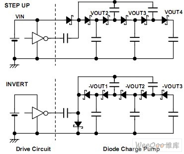
The basic circuit is as shown in figure 1.
The output voltage is as shown, the output voltage VOUT1, VOUT2, VOUT3 is the 1, 2, 3 times of the input voltage respectively. The rising voltage produces the N(>=2) times voltage by using the single power supply and the clock pulse; the reversal uses the clock pulse to produce the -N(>=1) times voltage.
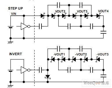
Figure 2 is the changed circuit, the rising time of it is shorter than the basic circuit, but the stability is poor.
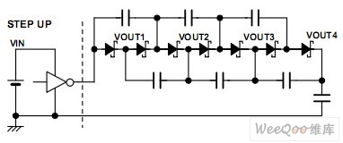
Figure 3 is the method which only uses the clock pulse to produce the rising voltage. Although you need to add some schottky diodes and capacitances in the circuit, but you do not need the single power supply.
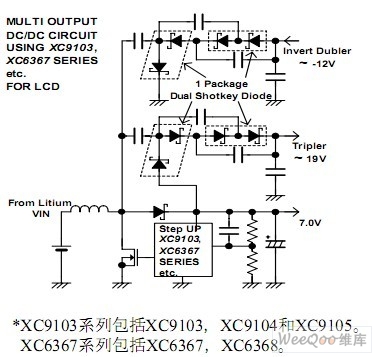
Figure 4 is the multi-power application example which is composed of the figure 3 circuit. This design can be used in the PDA and LCD applications, because this device can produce multiple groups of positive and negative voltage output by using a single channel DC/DC converter, such as the 9103 series.
Figure 1 The basic circuit 1
Figure 2 The basic circuit 2
Figure 3 The voltage rising circuit which uses the clock pulse only
Figure 4 The application example of the multi-power
Reprinted Url Of This Article:
http://www.seekic.com/circuit_diagram/Basic_Circuit/Charge_pump_multi_voltage_output_circuit_composed_of_Walter_Schottky_diodes.html
Print this Page | Comments | Reading(3)

Article Categories
power supply circuit
Amplifier Circuit
Basic Circuit
LED and Light Circuit
Sensor Circuit
Signal Processing
Electrical Equipment Circuit
Control Circuit
Remote Control Circuit
A/D-D/A Converter Circuit
Audio Circuit
Measuring and Test Circuit
Communication Circuit
Computer-Related Circuit
555 Circuit
Automotive Circuit
Repairing Circuit
Code: