
Circuit Diagram
Index 1650
Electrical blaster 3
Published:2011/6/28 2:44:00 Author:Nicole | Keyword: Electrical blaster

The electrical blaster circuit is composed of delay switch circuit, insurance switch circuit, timing detonating circuit, charge indication circuit and detonating power supply circuit, it is shown in the figure 8-25.
The delay switch circuit is made of time base integrated circuit IC1, resistors R1, R2, potentiometer RP1, potentiometers C1-C3, diode VD1, thyristor VT1 and the contact S2-1 of detonating switch S2.
The insurance switch circuit consists of time base integrated circuit IC2, resistors R3, R4, potentiometer RP2, diode VD2, VD3, capacitors C4, C5, relay K and the contact S2-2 of S2.
(View)
View full Circuit Diagram | Comments | Reading(712)
Electrical blaster 2
Published:2011/6/28 2:33:00 Author:Nicole | Keyword: Electrical blaster
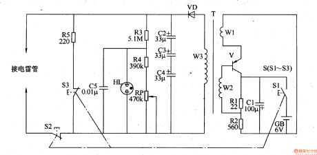
The electrical blaster circuit is composed of oscillator, boost circuit, charge indication circuit and discharge circuit, it is shown in the figure 8-24.
The oscillator is made of transistor V, capacitor C1, resistors R1, R2, battery GB, charge switch S1 and W1, W2 windings of boost transformer T.
The boost circuit consists of W3 winding of boost transformer T, rectifier diode VD and capacitors C2-C4.
The charge indication circuit is composed of resistors R3, R4, potentiometer RP, capacitor C5 and neon indication light HL.
The discharge circuit is made of discharge switch S2, drain switch S3 and resistor.
(View)
View full Circuit Diagram | Comments | Reading(916)
Consisting of uPC1378H field output circuit
Published:2011/6/28 3:14:00 Author:Fiona | Keyword: Consisting of uPC1378H, field output

uPC1378H pin functions:
1 pin : 0V - ground
2 pin : 12V - output field
3 pin : 26V - bootstrap voltage input
4 pin : 0.8V-- field drive signal input
5pin : 0V - external decoupling capacitor
6 pin : 26V - power input
7 pin : 1.8V-- bootstrap voltage output
(View)
View full Circuit Diagram | Comments | Reading(2531)
Loom saves electricity controller 6
Published:2011/6/29 22:16:00 Author:Nicole | Keyword: loom, saves electricity controller
The loom saves electricity controller circuit is composed of control switch S1, starter button S2, AC contactor KM, heat relay KP, relay K, resistor R, capacitor C, rectifier diode VD and microswitch S3, it is shown in the figure 8-22.
The control switch S1 is turned on, the starter button S2 is pressed, AC contactor KM is connected and pulled in, it is self-lock, the motor M is electrifying and running. The loom's machine open and shut down handle is set in start-up position, the microswitch S3's two groups normally closed contacts are turned on, the normally open contact cuts off.
(View)
View full Circuit Diagram | Comments | Reading(718)
Many files optional timer circuit
Published:2011/6/28 4:07:00 Author:Fiona | Keyword: Many files optional timer

SBl is the start switch, sB2 is the stop switch. When you press the start switch SB1, the DC power supply charges the capacitor c3 through R2, the potential of integrated operational amplifier A phase input 3 is higher than the potential of reverse phase input 2, A outputs a high potential to trigger the directional Triode Thyristor VS to make the V5 conduct.AC power adds to electricity load through VS,timing power supply begins.After the release of SB1,C3 discharges by the A phase input,the length of discharging time depends on the c3's capacity,the resistance of resistors R6-R9 and the discretion of A reverse end (2) potential.
(View)
View full Circuit Diagram | Comments | Reading(857)
555 Square wave Generator with a Large-scale Changeable Duty cycle
Published:2011/6/30 0:04:00 Author:Zoey | Keyword: 555 quare wave Generator, Large-scale Changeable, Duty cycle
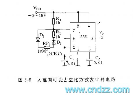
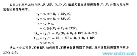
Figure 3-5 Square wave Generator Circuit with a Large-scale Changeable Duty cycle
As shown in the figure 3-5, 555, R1,R2, RP1, D1,D2 and C1 constitute an astable multi-vibrator. D1 and D2 refer to the guide tubes on the charge and discharge loop respctively.
tc=0.693(R1+RPleft)C1
td=0.693(R2+RPright)C1
t=tc+td
=0.693(R1+R2+RP)C1
Dmin=tc/T=(R1+R2+RP)≈0.01%
Dmax=tc/T=(R1+RP)(R1+R2+RP)
≈99.99%
From the formula above we can conclude that, no matter how RP1 is adjusted to, the oscillation period won't be affected. Oscillation frequency of the parameter in the figure is about 20Hz.
(View)
View full Circuit Diagram | Comments | Reading(805)
Luminous Logic Pen Circuit Diagram
Published:2011/6/16 10:58:00 Author:Vicky | Keyword: Luminous Logic Pen

Logic pen is also called as logic test probe, which is a commonly-used tool in testing the logic states of the dots in a digital circuit. The logic states in a digital circuit can be divided as high level ‘1’, low level ‘o’ and high impedance state (infloating). The test results of the logic states can be displayed by a luminous diode, or an acoustical generator, or a digital luminous diode. The above picture is a logic test pen composed of hex-inverter CD4069 and luminous diode. (View)
View full Circuit Diagram | Comments | Reading(890)
Sound-Type Logic Pen Circuit Diagram
Published:2011/6/16 10:57:00 Author:Vicky | Keyword: Sound-Type Logic Pen
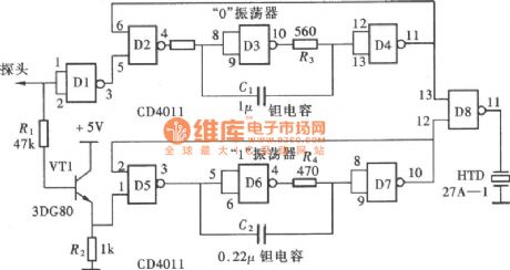
The result of sound-type logic pen is observed by naked eyes. Due to the high development of modern electronics producing technology, soldered dots are densely assigned in the circuit board. Therefore when testing, one should concentrate on it and his eyes should always focus on the tested dot. Hence if a sound-type tester is made, our ears can be also used in testing and it will highly improve the efficiency. The above picture ia the sound-type logic pen composed of NAND gate CD4011. (View)
View full Circuit Diagram | Comments | Reading(683)
Metal Detector (MC14046-B) Circuit Diagram
Published:2011/6/23 8:42:00 Author:Vicky | Keyword: Metal Detector Circuit

Metal Detector is shown in the above picture. Detection coils constitute the LC oscillating circuit. When the coil gets close to the metal, the metal will generate eddy current inside, change the amount of coil inductance and thereby change the oscillating frequency of the detector circuit. Picture(a) is the functional block diagram of the detector and picuture(b) is the detecting picture. (View)
View full Circuit Diagram | Comments | Reading(3395)
Control voltage phase shifting trigger circuit
Published:2011/6/27 7:20:00 Author:Christina | Keyword: Control voltage, phase shifting, trigger circuit

As the figure shows, this circuit uses the semiconductor transistor instead of the charging resistance R, and this circuit adds the control voltage Vi on the base electrode of the transistor, when the Ui changes, the collector electrode current IC of the VT1 will change too. When the IC increases, the trigger pulse moves forward; when the IC decreases, the trigger pulse moves backward to achieve the purpose of the phase shifting.
Control voltage phase shifting trigger circuit (View)
View full Circuit Diagram | Comments | Reading(514)
Complementary oscillator trigger circuit
Published:2011/6/27 7:26:00 Author:Christina | Keyword: Complementary oscillator, trigger circuit
The circuit is as shown in the figure. The positive feedback loop is composed of the VT1 and VT2 to produce the self-excited oscillation triggering pulse, you can change the cycle of the self-excited oscillation triggering pulse by adjusting RP, and this circuit plays the role of phase shifting.
Complementary oscillator trigger circuit (View)
View full Circuit Diagram | Comments | Reading(516)
Neon light trigger circuit
Published:2011/6/27 7:51:00 Author:Christina | Keyword: Neon light, trigger circuit
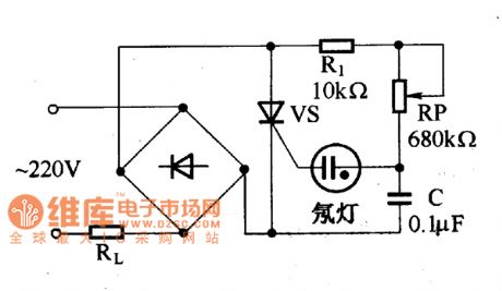
The circuit is as shown in the figure, it is composed of the R1, RP, C and the neon light. The general neon light can puncture the conduction with the voltage of 60 to 90V, we can form the relaxation oscillator by using this feature, and this relaxation oscillator produces the pulse to trigger the thyristor to adjust the voltage. When the voltage of the capacitor is charged to the neon light's striking voltage, the neon light is punctured, the voltage of capacitance C discharges to the control electrode of the thyristor, and the trigger thyristor conducts. After the voltage of capacitance C discharges, the neon light turns off and the power recharges the C. So we can get a series of trigger pulses.
Neon light trigger circuit (View)
View full Circuit Diagram | Comments | Reading(616)
Single phase bridge type thyristor rectifier circuit
Published:2011/6/27 8:04:00 Author:Christina | Keyword: Single phase, bridge type, thyristor, rectifier circuit
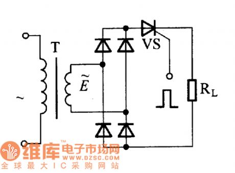

The single phase bridge type thyristor rectifier circuit is composed of the single phase bridge type rectifier circuit, the unidirectional thyristor and the load RL, as the figure shows. The single phase AC voltage is bridge-type rectified by this circuit and becomes the full-wave rectifier waveform. Because only when the trigger signal increases, the thyristor will conduct, and the thyristor is cut off when the AC voltage is crossing zero, so we can get the waveform which is as shown in figure (5). From the figure a and b, we can see that when the angle θ is small, the DC voltage average values at both ends of the load resistanceare small; when the angle θ increases, the DC voltage average values of the load resistanceare high.
(View)
View full Circuit Diagram | Comments | Reading(3787)
Three-phase bridge type thyristor rectifier circuit
Published:2011/6/27 7:37:00 Author:Christina | Keyword: Three-phase, bridge type, thyristor, rectifier circuit
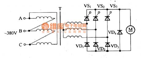
The three-phase bridge type thyristor rectifier circuit is as shown in the figure. The difference between this circuit and the three-phase bridge type rectifier circuit is: this circuit uses the unidirectional thyristor to replace the three rectifier diodes of the half bridge arm. You can change the thyristor conduction time of every cycle by changing the conduction angle θ of the three thyristors, and you can get the adjustable DC voltage average value. The three-phase bridge type thyristor rectifier circuit can be used in the speed regulation device of the high power DC motor.
Three-phase bridge type thyristor rectifier circuit (View)
View full Circuit Diagram | Comments | Reading(2258)
Partial voltage type negative feedback bias circuit
Published:2011/6/27 21:36:00 Author:Christina | Keyword: Partial voltage, negative feedback, bias circuit
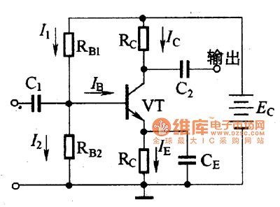
This circuit is designed as one kind of bias circuit, the typical circuit is as shown in the figure. In this circuit, the transistor emitter is connected with the RE, and the base electrode is connected with the RB1 and RB2.
Figure Partial voltage type negative feedback bias circuit
The partial voltage type negative feedback bias circuit has two kinds of stable effects:
1. Through the partial voltage of the base resistance RB1 and RB2, this relation is founding:
I2=I1-IB≈I1
UB=Ec-I1RB1
UB=I2xRB2
2.If you add the RE in this circuit, this circuit will have the function of current negative feedback temperature compensation.
Because of the two stable functions, this partial voltage type negative feedback bias circuit has good stable function. (View)
View full Circuit Diagram | Comments | Reading(597)
Current negative feedback bias circuit
Published:2011/6/28 1:29:00 Author:Christina | Keyword: Current, negative feedback, bias circuit
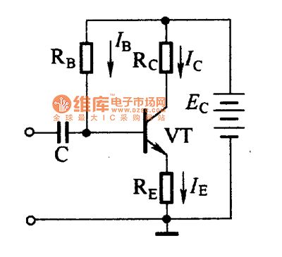
The current negative feedback bias circuit is as shown in the figure. The difference between this circuit and the fixed bias circuit is the semiconductor transistor emitter is connected with a resistance RE. The parameters of this circuit are: Ec=IERE+UBE+IBRB.
As the EC power is constant, if the IERE increases, the UBE will decreases, so the IB decreases too. The process of the circuit stable quiescent operating point is:
↑-->Ic↑-->IE↑-->IERE↑-->UBE↓-->IB↓-->IC↓
Figure: Current negative feedback bias circuit
(View)
View full Circuit Diagram | Comments | Reading(738)
Smoke alarm circuit
Published:2011/6/28 2:58:00 Author:Christina | Keyword: Smoke, alarm
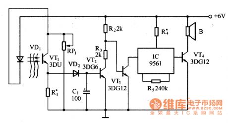
The smoke alarm circuit is composed of the infrared light tube, the series feedback photosensitive circuit (composed of the phototransistor), the semiconductor tube switch circuit and the integrated alarm circuit, as the figure 8 shows. When the monitored environment has no smoke, the infrared light-emitting diode VD1 lights with the pre-tuned initial current. This infrared light is received by the photosensitive transistor VT1 to reduce the resistance of VT1 amd increase the current of VD1 and VT1, so the luminous intensity of the infrared light-emitting diode VD2 increases accordingly.
Figure: Smoke alarm circuit (View)
View full Circuit Diagram | Comments | Reading(585)
Loom saves electricity controller 5
Published:2011/6/29 22:05:00 Author:Nicole | Keyword: loom, saves electricity controller

The loom saves electricity controller circuit is composed of knife switch Q, fuse FU, stop button S1, starter button S2, microswitch S3, time relay KT, AC contactor KM, heat relay KP and motor M, it is shown in the figure 8-21.
The knife switch Q is connected, starter button S2 is pressed, AC contactor KM is turned on and pulled in, motor M starts running. When the machine open and shut down handle is in start-up position, microswitch S3 is in off state, time relay KT is in release state.
(View)
View full Circuit Diagram | Comments | Reading(539)
Infrared ray alarm circuit
Published:2011/6/30 3:38:00 Author:Christina | Keyword: Infrared ray, alarm
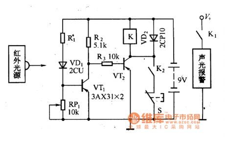
The infrared ray alarm circuit is as shown in the figure. It is composed of the light source, the receiver and the sound and light alarm circuit. There is the infrared receiver in a certain distance from the infrared light source, so there is an invisible infrared cordon between the infrared light source and the receiver.
When no one keeps out the infrared ray, the infrared ray irradiates on the photosensitive diode VD1 directly, so the photosensitive diode's resistance becomes smaller to conduct the VT1, the VT2 is in the cut-off state, the relay K which is connected with the collector VT2 will not work, the contact point K1 opens, so the sound and light alarm system has no power voltage to work.
Figure The Infrared ray alarm circuit (View)
View full Circuit Diagram | Comments | Reading(625)
Infrared remote control switch circuit
Published:2011/6/29 5:59:00 Author:Fiona | Keyword: Infrared remote control switch
The remote control transmitter which is used is ordinary home appliance remote control.Receiveing control circuit is welded according to the figure,it can be successful without debugging.IR is infrared remote control receiving head,when the infrared signal is not received,① pin outputs the high level;when the infrared signal is received,① pin outputs a series of low level pulse.R4,C2 and R7,C3 compose two integrating circuit, Q4, Q5.J compose the relay control circuit.C5, D5 ~ D8 compose exchange step-down rectifier circuit.Usually original state after standby or power up is:Q1 conducts,Q2 is closed,Q5 is closed,the relay J does not work.
(View)
View full Circuit Diagram | Comments | Reading(963)
| Pages:1650/2234 At 2016411642164316441645164616471648164916501651165216531654165516561657165816591660Under 20 |
Circuit Categories
power supply circuit
Amplifier Circuit
Basic Circuit
LED and Light Circuit
Sensor Circuit
Signal Processing
Electrical Equipment Circuit
Control Circuit
Remote Control Circuit
A/D-D/A Converter Circuit
Audio Circuit
Measuring and Test Circuit
Communication Circuit
Computer-Related Circuit
555 Circuit
Automotive Circuit
Repairing Circuit