
Circuit Diagram
Index 1644
Automobile Steering Flasher (6)
Published:2011/6/30 6:00:00 Author:Sue | Keyword: Automobile, Steering, Flasher
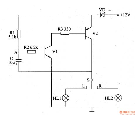
When S is put on L or R , +12V voltage will be put on V2. The other circuit will charge C by VD and R1. When C's voltage reaches a certain value, V1 and V2 will be connected. The left turn lamp HL1 or right turn lamp HL2 will be illuminated. After V2 is connected, C will be discharged by V2,VD. V1,V2 will be connected. HL1, HL2 will be off. Then C will be charged by R1 which will make V1,V2 connected. The circuit keeps on working like this. (View)
View full Circuit Diagram | Comments | Reading(515)
Automobile Steering Flasher (5)
Published:2011/6/30 5:54:00 Author:Sue | Keyword: Automobile, Steering, Flasher

S is the turn lamp switch. HL1 is the left turn lamp switch. HL2 is the right turn lamp switch.
The astable multivibrator will generate low-frequency oscillate signals which will be put on V3. When S is put on L or R , V3 will be connected intermittently, which will make HL1 or HL2 illuminated with a twinkle frequency of70-75 times/min. (View)
View full Circuit Diagram | Comments | Reading(546)
Automobile Steering Flasher (4)
Published:2011/6/30 5:50:00 Author:Sue | Keyword: Automobile, Steering, Flasher
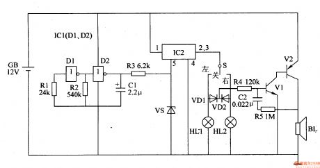
The low-frequency oscillator will generate 1Hz pulse signals which will control HL1 and HL2.
IC2's inner switch will be connected intermittently under the control of the signals. When the pulse signals are positive, IC2's inner switch will be connected. When the signals are negative, IC's inner switch will be disconnected.
When S is put on LEFT , the left turn lamp HL1 will be illuminated and VD1 will be connected intermittently. The indicator will begin to work and BL will make a warning tone. When S is put on RIGHT , the right trun lamp HL2 will be illuminated and VD2 is connected intermittently. The indicator will begin to work. When S is put in middle, HL1 and HL2 are both off and VD1,VD2 are both disconnected. The indicator doesn't work and BL makes no sound. (View)
View full Circuit Diagram | Comments | Reading(445)
Automobile Steering Flasher (3)
Published:2011/6/30 5:42:00 Author:Sue | Keyword: Automobile, Steering, Flasher
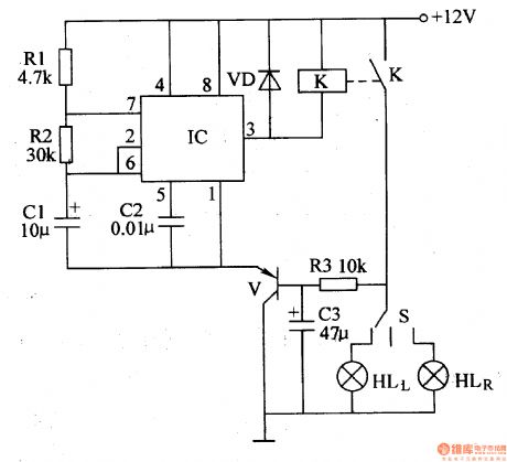
When S is disconnected, V is disconnected. IC's pin 1 and pin 3 will output high level while the oscillator doesn't work. When S is connected, V is connected. IC's pin 1 will output low level. The oscillator begins to work. IC's pin 3 will output oscillate signals which will make K connected and disconnected intermittently. HLL or HLR will be illuminated simultaneously. When S is put in the middle, V is disconnected. The oscillator will stop working. The turn lamps will be off. (View)
View full Circuit Diagram | Comments | Reading(483)
Automobile Steering Flasher (2)
Published:2011/6/30 5:36:00 Author:Sue | Keyword: Automobile, Steering, Flasher

When S2 is connected, +V will provide the square wave oscillator with working power after limitation and stablization. When the oscillator begins to work, it will generate 1Hz square wave oscillate signals which will make V1 connected intermittently and the turn lamp will begin to twinkle. When the square wave signals are positive, V1 is connected and K is connected. HL1, HL2 or HL3, HL4 will be illuminated. When the square wave signals are negative, V1 is disconnected and K is released. The turn lamps will be off.
+V will provide IC2 with 3V working voltage after stablization. After IC2 is connected, music will be generated. (View)
View full Circuit Diagram | Comments | Reading(445)
Automobile Steering Flasher (1)
Published:2011/6/30 5:29:00 Author:Sue | Keyword: Automobile, Steering, Flasher
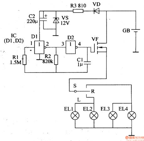
S is the steering switch, and EL1 is left frontturn lamp, EL2 is left rear turn lamp, EL3 is right front turn lamp while EL4 is right rear turn lamp. GB is the storage battery of the automobile.
GB will provide VF with working voltage. The other circuit will provide IC with +12V voltage after limitation, stablization and filtration.
After the multivibrator begins to work, IC's pin 4 will output low-frequency square wave pulse signals. When S is connected, VF will be connected and disconnected intermittently. Then EL1,EL2,EL3,EL4 will start to twinkle. When VF is connected, the turn lamps will be illuminated. When VF is disconnected, the turn lamps will be off. (View)
View full Circuit Diagram | Comments | Reading(546)
Fluorescent Lamp Electronic Ballast (4)
Published:2011/6/26 5:31:00 Author:Sue | Keyword: Fluorescent Lamp, Electronic, Ballast

When the power is on, the 220v voltage will provide the oscillator with 300v working voltage after filtration and rectification.
The moment the power is on, one of V1 V2 is connected and V1 V2 will be connected intermittently. The oscillate circuit will be auto-excited. EL will be provided with voltage. When the voltage reaches the discharging voltage of EL, EL will be illuminated. (View)
View full Circuit Diagram | Comments | Reading(3081)
Fluorescent Lamp Electronic Ballast (3)
Published:2011/6/26 5:23:00 Author:Sue | Keyword: Fluorescent Lamp, Electronic, Ballast

When the power is on, the 220v voltage will provide the oscillate circuit with 300v working voltage after filtration and rectification. It will charge C2 by R1 and when the voltage reaches a certain value, V3 is connected and the oscillate circuit begins to work. V1 and V2 are connected and EL will be provided with working voltage which will illuminate EL. (View)
View full Circuit Diagram | Comments | Reading(4663)
56~484 High Frequency Oscillator Circuit
Published:2011/6/21 3:54:00 Author:Joyce | Keyword: 56~484, High Frequency , Oscillator
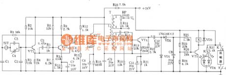
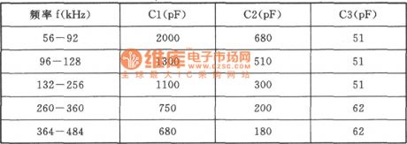
As shown in the figure is a high frequency oscillator, which can be used as an exclusive high frequency generator. Different values of capacitance will produce a high frequency sine wave in the range between 56 to 484 kHz. This circuit has the characteristics of good waveform, high frequency stability, and low output impedance and so on.
Choice of components:
Transistor VT1, VT2: 3 DG6D, 65≤β≤115, VT3、 VT4:3 DG 1308, 60≤β≤85. Semi-adjustable capacitors C4: CCWX-3-5/20 pF. Quartz crystal SJT: BE-42. K: JZX-10 M (miniature relay). Light emitting diode VD4: BT-605 (red, green). Transformer T: MXD-2000 ferrite, GV- 30x 19magnetic core.DLL-2. Φ 0.21 mm high strength enameled wire, rolled in 133 turns, L3-4 Φ0.21 mm high strength enameled wire rolled in 11 turns , L5-6 Φ0.21 mm high strength enameled wire, rolled in 80 turns. Except resistance R27 which adopts l/2WRJ , all the other resistance use 1/8 WRJ.
The relationship between the frequency and capacitance values are shown in the following figure.
(View)
View full Circuit Diagram | Comments | Reading(628)
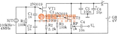
VR-tube High Frequency Signal Generator Circuit
Published:2011/6/30 2:51:00 Author:Joyce | Keyword: VR-tube , High Frequency , Signal , Generator
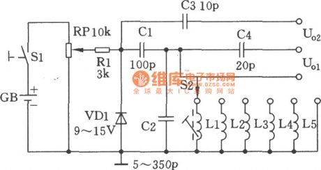
As shown in figure, the circuit uses the characteristic of zener breakdown of the VR-tube to get high frequency signals amounting to hundreds of megahertz. Single frequency signals from the output end V01 can be used to adjust the resonant frequency of the tuning circuits. High frequency signals of broad spectrum from output end V02 can track between the input resonant circuits and the local oscillator tuning circuit of uperheterodyne resonant receiver. The frequency range of the generator is 100kHz ~ 27 MHz, which is divided into five frequency range :100kHz~300kHz~1MHz~3MHz~9MHz~27MHz. (View)
View full Circuit Diagram | Comments | Reading(2063)
High-Frequency-Generating Lamplighter Circuit
Published:2011/6/30 3:21:00 Author:Joyce | Keyword: High-Frequency-Generating , Lamplighter

As shown in the figure is a high-frequency-generating lamplighter circuit. Supplied by battery of 8 V ~ 14 V, it will light 6 W ~ 12 W fluorescent lamps after oscillation. Transistor VT can use low frequency high power transistor like 3DD12A, D3D4D, 3 DD5C and 3 DDl5.When in assembly, aluminum radiator of 70mm×40mm×2mm shall be installed; Small wire-round potentiometer RP would be first choice; High-frequency pulse transformer T can use ferrite cans of 22 mm in diameter. (View)
View full Circuit Diagram | Comments | Reading(1293)
Collpitts Oscillator Circuit
Published:2011/6/21 3:33:00 Author:Joyce | Keyword: Collpitts , Oscillator
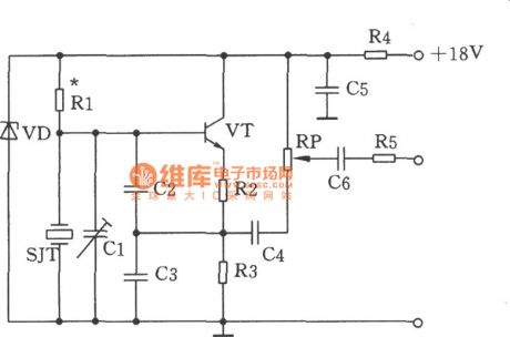
As shown in the figure is a colpitz oscillator circuit. It has a crystal with fundamental frequency of 1499 kHz. Crystal SJT is connected at the ends of capacitance C2 and C3 in parallel. Emitter divider resistances R2, R3 will provide basic feedback signals, which are controlled by capacitance dividers C2 and C3. After crystal SJT starts oscillation, it will transfer sine signals of 1499 kHz to audion VT base, and the signals will be output through emitter follower VT. Then they will go through coupling capacitance C4 to potentiometer RP. Resistance R1 would give a suitable offset voltage to VT by depressing the 18 V voltage. (View)
View full Circuit Diagram | Comments | Reading(607)
Multiple-frequency Signal Generator Circuit
Published:2011/6/30 3:34:00 Author:Joyce | Keyword: Multiple-frequency , Signal, Generator

As shown in the figure is a multi-frequency signal generator. SJT, VT1 constitute a crystal oscillator. Since quartz crystal SJT is used as an equivalent inductance, which has a high equivalent value Q, other components and stray parameters have little effect on the oscillation frequency, therefore it has a stabile frequency. Source follower is composed of VT2 to get lower output impedance and buffering, so as to avoid effect on the stability of crystal caused by loading. In order to obtain more frequency marks to calibrate the receiver, the following square wave circuit can be used.
(View)
View full Circuit Diagram | Comments | Reading(1159)
Mutiple Waveform Generator Circuit
Published:2011/6/30 3:48:00 Author:Joyce | Keyword: Mutiple , Waveform , Generator

As shown in the figure, the circuit can produce and output square wave, triangle wave and sine wave.It is especially suitable for electronic lovers and students doing experiments with oscilloscopes to observe the signal waveform. This signal generator circuit is simple, low-cost and easy to adjust. 555 timing is connected in a multivibrator form. C2 is a timing capacitance, whose charging loop and discharging loop is R2→R3→RP→C2 and C2→RP→R3→ foot 7 of IC(discharge tube) respectively. Because R3+RP》R2 , the charging time constant and discharging time constant are approximately equal. Output of foot 3 of IC is approximately symmetric square wave. (View)
View full Circuit Diagram | Comments | Reading(3160)
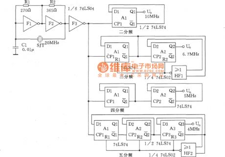
Mutiple Output Crystal Oscillator Circuit
Published:2011/6/30 3:58:00 Author:Joyce | Keyword: Mutiple Output, Crystal, Oscillator

As shown in the figure is a multiple output crystal oscillator. It is mainly composed of 3 gates of Al, four resistances, two capacitances and a piece of crystal. R1 ~ R4 offset two inverters within the linear range, and they are connected between foot 4 and foot 1 of A1 by crystal SJT to provide the feedback loop. It will produce oscillation only on the fundamental frequency of the crystal.
Choice of components: capacitance C1 is 15 p (fine-tuning capacitor). Resistance R1, R3 is 220 Ω, R2 is 560 Ω, R4 is 1.8 k Ω, R5 is 1 kΩ, and the nominal power is 1 / 8 W. Integrated circuit Al is 7404, A2 is 74 LS74, and A3 is 74 LS393. Quartz crystal SJT is SW60A-4096 kHz. Switch SA is KNX (1 x 3). (View)
View full Circuit Diagram | Comments | Reading(1361)
AC power detecting circuit made by MD7750
Published:2011/6/21 8:10:00 Author:leo | Keyword: AC power detecting circuit made by MD7750, AD7750

As picture a and b show, this is a AC power detecting circuit made by MD7750.AC power is the product of multiplication of current value and voltage value. This circuit is used to detect the power of 50 Hz single phase AC circuit. It can adopt common A/D converter but here it takes special A/D converter AD7750 with power detecting function.
The voltage value and current value can be tested on the high voltage terminal, therefore, current and voltage signals can be detected by voltage divider.AD7750 has two input terminals which are current signals terminal V1 and voltage signals terminal V2. These two terminals are different from each other. (View)
View full Circuit Diagram | Comments | Reading(627)
Square Wave and Sine Wave Generator Circuit
Published:2011/6/30 4:08:00 Author:Joyce | Keyword: Square Wave , Sine Wave , Generator

As shown in the figure is a square wave and sine wave generator. A clock generator is composed of an ordinary inverse gate and a few components only, which can output two waveforms of the same frequency at the same time: square wave and sine wave. The oscillator operates well in the frequency range between 100 Hz and 10 MHz. If 74 HCU00 which has no buffering output level is used instead of 74 HC00, it will achieve a better effect. (View)
View full Circuit Diagram | Comments | Reading(4932)
Crystal Oscillator and Frequency Divider Circuit
Published:2011/6/30 4:10:00 Author:Joyce | Keyword: Crystal Oscillator, Frequency Divider
View full Circuit Diagram | Comments | Reading(1624)
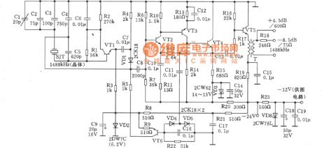
1488kHz Signal Generator and Frequency Divider Circuit
Published:2011/6/30 4:12:00 Author:Joyce | Keyword: 1488kHz, Signal Generator , Frequency Divider
View full Circuit Diagram | Comments | Reading(1052)
VCT3803-O1A-Super TV single chip integrated circuit
Published:2011/6/17 7:44:00 Author:leo | Keyword: VCT3803-O1A-Super TV single chip integrated circuit, TDA4472, MSP3463G

VCT3803-O1A is a kind of super TV single chip integrated circuit used in German which is widely used in big screen color television.1. Function Features:VCT3803-O1A contains micro processor, TV/AV converting circuit, brightness signal processing circuit, color signal demodulating circuit, BGR square circuit, BGR signal selecting switch circuit and so on.2.Pin Functions and data:VCT3803-O1A is used in P2960S KangJia series color television and its pin functions and data are shown in the picture. (View)
View full Circuit Diagram | Comments | Reading(947)
| Pages:1644/2234 At 2016411642164316441645164616471648164916501651165216531654165516561657165816591660Under 20 |
Circuit Categories
power supply circuit
Amplifier Circuit
Basic Circuit
LED and Light Circuit
Sensor Circuit
Signal Processing
Electrical Equipment Circuit
Control Circuit
Remote Control Circuit
A/D-D/A Converter Circuit
Audio Circuit
Measuring and Test Circuit
Communication Circuit
Computer-Related Circuit
555 Circuit
Automotive Circuit
Repairing Circuit