
Circuit Diagram
Index 1648
oscillator composed of gate circuit circuit
Published:2011/6/26 8:36:00 Author:Fiona | Keyword: composed of gate circuit
View full Circuit Diagram | Comments | Reading(512)
Parallel type crystal oscillator circuit
Published:2011/6/26 9:01:00 Author:Fiona | Keyword: Parallel type, crystal
Among this circcuit, the resistors R1,2 and resistors R5, R6, R7 are the DC bias component of the transistors VT1 and VT2.High-frequency choke coil L2 offers the DC path to the the collector current of the oscillation tube VT1. C2 is the blocking capacitors.C3, C7 are the exchange bypass capacitor which make the emitter of the VTl in exchange zero potential,but the DC-bit is not zero.The inductor L1, capacitor c6,resistor R 3 improve the power supply filter circuit,whose role is to reduce ripple voltage to increase the DC component. Slightly adjustable capacitors can change the size of the coupling signal.
(View)
View full Circuit Diagram | Comments | Reading(515)
Inductance Tuning Crystal Radio Circuit
Published:2011/6/28 6:08:00 Author:Michel | Keyword: Inductance Tuning Crystal Radio Circuit
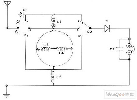
First of all,the Q value of the spherical adjustable inductance coil is measured by Q table. the capacitor The capacitor of Q table is fixed on 55pf and the measuring result is:Maximum induction:550 KHz Q = 68,Middle induction:745 KHz Q = 60,Minimum induction:2770 KHz Q = 30.The capacitor of Q table is fixed on 80 pf and the measuring result is:Maximum induction:478 KHz Q = 77,Middle induction:995 KHz Q = 47,Minimum induction:2300 KHz Q = 15.
The coil's Q value is not high,especially the inside and outside coil reverse and the Q value is lower when the inductance cancel each other out.But it can used as crystal radio receiver tuning without variable capacitor and the line is simpler. (View)
View full Circuit Diagram | Comments | Reading(1408)
1.5 Km Single Pipe FM Launching Circuit
Published:2011/6/22 5:04:00 Author:Michel | Keyword: 1.5 km, Single Pipe, FM, Launching Circuit

This circuit is 1.5 km single pipe FM (FM)emitting circuit.Emitting triode uses D40,D50 and 2N3866 and the work current is 60-80mA.But the aboved triode is hard to buy and the price is high and fakes are more.The author chooses other transistor to make experiments and the C2053 and C1970 is rather good.The actual horizon communication distance is over 1.5km.The author also has had changed the D40 tube into ordinary transistor 8050,its work current is 60~80mA but the emitting distance is less than 1.5m.If it is altered into 9018,the work current is much lower and the launching distance is shorter. (View)
View full Circuit Diagram | Comments | Reading(602)
Module Super-regenerative FM Radio Cirucit of Electron Tube
Published:2011/6/22 5:00:00 Author:Michel | Keyword: Electron Tube, Module Super-regenerative, FM Radio Cirucit

Devices Selection
The machine circuit is shown in the picture and it is a superregenerative receiver circuit.Because most channel frequencies work between 88MHz~108MHz and take Shanghai literature and art channel (the middle frequency is 96.8MHz)as example.L2 uses Φ2mm silver-coated copper wire.On the diameter Φ15mm mould,it can be roped into 5 circles hollow type whose coil distance is 2mm. The distances between two circles is about 2mm-3mm.The radio frequency choke uses Φ0.32mm lacquered wire.The diameter 10mm paper tube is raped into 150 circles which is divided into three sections hives and the distance is 2mm. (View)
View full Circuit Diagram | Comments | Reading(7068)
Super-regenerative Wirless Receiving Circuit
Published:2011/6/22 4:56:00 Author:Michel | Keyword: Super-regenerative, Wirless, Receiving Circuit

The receiver can use super regenerative circuit or tropadyne and the power consumption is 100uA.The adjustable super regenerative circuit's sensitivity is similar to first level oscillating,mixing and two-stage superheterodyne receivers.However,super regenerative circuit's work stablity and selection performance are not good which decreases anti-Impacting performance.The picture is typical tropadyne. (View)
View full Circuit Diagram | Comments | Reading(1664)
Wireless FM Emitting Circuit of 3000 Meters Launching Distance
Published:2011/6/22 4:51:00 Author:Michel | Keyword: 3000 Meters, Launching Distance, Wireless FM, Emitting Circuit


The work voltage and current are 9V and 2~6mA respectively and the element's parameters are shown as the aboved picture.BG1 is 9018,BG2 is C1959(It can be 9018 but the power is low.If the D-40 can spread the emitting distance to 1000m and it's hard to buy D-40 in shops).L1 and L2 are 0.5mm lacquered wires and the work voltage can be increased to 12V when we loope four and three circles on the 0.5 round bars.Thus the emitting distance can be increased but the frequency will change.At this time,it's better for the whole circuit uses battery charging to reach optimal results of quality and stable frequency and please turn off BG2 work and needed frequency when you start debugging and turn on BG2 circuit's adjustable power at last.
(View)
View full Circuit Diagram | Comments | Reading(621)
Electronic timer switch circuit
Published:2011/6/27 2:52:00 Author:Fiona | Keyword: Electronic timer, switch

Close the power switch sA,the LED vD2 indicates the work,reduces the voltage by limiting resistor R2 and capacitance c1,rectifys by diode VD3,then filters by balanced symmetrical capacitance c2—c7 and obtains the 6v DC voltage in C7 ends.Because the backward resistance of the emitter junction is large and the input resisters of transistors VTl,VT2,VT3 are connected,The resistance is also very large,so this circuit can increase regular time.When turn on the power,the capacitor c8's voltage is Uc8 = oV, vTl, vT2, VT3 are cut off.vT4 provides the constant charging electric current to C8to make the Uc8 hasten linear growth.
(View)
View full Circuit Diagram | Comments | Reading(834)
the temperature controller circuit(11)
Published:2011/6/30 8:30:00 Author:Ariel Wang | Keyword: temperature, controller
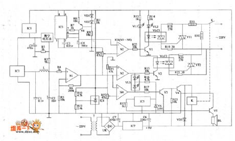
The 220V AC voltage is reduced by T.It is commutated by UR.It is filtered by C7 and regulated by IC7.It provides +9V working voltage for the saw-toothed wave generator, the pulse-width-controllable circuit ,the comparative amplification circuit,the executive and control circuit and the over thermal shutdown circuit.At this time,V4 is saturated to conduct.K is conducted to pull in.The normally open contacts are connected.The +9V voltage becomes +5V as it is regulated twice by IC1.It is the working power supply for IC2 and the digital voltmeter.IC2 converts the detected temperature signal to the voltage signal.After it is filtered by C2,L and C2,one part of the voltage is branched by R2 and R3.The digital voltmeter displays the temperature.The other part is amplified by N1.Then it is the sampling voltage for operational amplifier N2~N4.
(View)
View full Circuit Diagram | Comments | Reading(533)
Channel Selection and FM Circuit of TDA70887 Computer
Published:2011/6/28 6:12:00 Author:Michel | Keyword: TDA70887 Computer, Channel Selection, FM, Circuit

Channel Selection and FM Circuit of TDA70887 Computer (View)
View full Circuit Diagram | Comments | Reading(1561)
Low Cost Wireless Transmission Power Test Pen Circuit
Published:2011/6/22 5:44:00 Author:Michel | Keyword: Low Cost, Wireless Transmission, Power, Test Pen Circuit

I make some testing tools according to my over 20-year wireless work experience and one effective handset interphone transmission power test pen circuit is shown as the picture.If it is installed inside the multimeter's pen, as long as we make stylus approach to interphone's antenna top.And we can judge whether the interphone has transmission power or not accurately by the LED,D2's lightness and judge emitting power magnitude roughly according to LED's lightness and darkness degree.And its production cost is no more than RMB one yuan. (View)
View full Circuit Diagram | Comments | Reading(915)
Cage Type Motor Stator Resistance Step-down Start Control Circuit
Published:2011/6/28 6:15:00 Author:Michel | Keyword: Cage Type, Motor Stator, Resistance Step-downStart Control Circuit

Cage Type Motor Stator Resistance Step-down Start Control Circuit (View)
View full Circuit Diagram | Comments | Reading(1614)
Isolated Industry Control Voltage Output Circuit of AD5562
Published:2011/6/22 6:10:00 Author:Michel | Keyword: Isolated Industry , Control Voltage, Output Circuit

This circuit's industrial control output module provides a complete solution scheme.This design is applied to PLCs which needs dual output voltage and DCSes.AD5662 is a 16-bit 5 V power supply and SOT-23 encapsulation digital-to-analog converter.ADuM1401 four channel digital isolatior provides all signal isolation between micro controller and digital-to-analog converter.The circuit is complete with the external protection standard of IEC 61000 specifications by test and verification. (View)
View full Circuit Diagram | Comments | Reading(570)
555 continuous recording keeping sound control circuit
Published:2011/6/16 1:47:00 Author:TaoXi | Keyword: 555, continuous recording, keeping, sound control

As the figure 14-9 shows, the sound control circuit uses the 555 as the core, the monostable delay circuit is composed of the 555 and R2, C3. The recording signal gets into the circuit from port A, when there is no signal, VT1 cuts off, pin-6 has the high electrical level to reset 555, pin-3 outputs the low electrical level, VT2 cuts off, the motor M stops working, the circuit will not tape. When port A has the signal, the signal is amplified and rectified by D1, D2 and C2, the VT1 conducts, pin-2 has the low electrical level, 555 sets, VT2 conducts, the motor M starts working, the circuit will start taping. When there is no recording signal in a short time, the 555 will not reverse immediately, only when the C3 is charged to the 2/3VDD of pin-6 through R2, the 555 resets, pin-3 has the low electrical level, the delay time td=1.1R2C3, it is about 5 seconds.
(View)
View full Circuit Diagram | Comments | Reading(466)
555 eight stages touch volume controller circuit
Published:2011/6/16 1:32:00 Author:TaoXi | Keyword: 555, eight stages, touch, volume controller
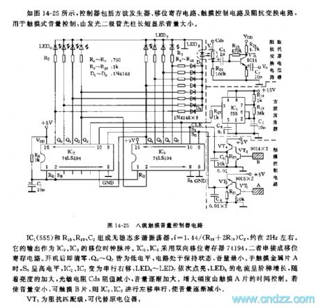
As the figure 14-25 shows, the controller is composed of the square wave generator, the shift register circuit, the touch control circuit and the impedance converting circuit, this controller can be used in the touch volume control, and it displays the volume by the LED light beam.
The astable multivibrator is composed of the IC1 (555) and R18, R19, C2, f=1.44/(R18+2R19)C2, it is about 2Hz. The output of it can be used as the shift clock pulse of the IC2 and IC3. The IC2 and IC3 use the two-way shift register 74194. The Q0-Q7 have the low electrical level, the circuit is in the keep state, the volume is minimum. When the hand touches the sheetmetal A, S0 has the high electrical level, IC2 and IC3 change into the serial right shift, the LED0-LED7 turns on one by one.
(View)
View full Circuit Diagram | Comments | Reading(1103)
The door control,light-dependent control switch circuit
Published:2011/6/27 23:45:00 Author:Fiona | Keyword: The door control, light-dependent control

When opens the door,the contact of the key switch SB is closed.The city power reduces voltage by the capacitor C1,rectifys by the diode VDl,indicator light LED is lit.At the same time,the city power reduces voltage by c2,then outputs 12v dc voltage by c3 after filtering. During the day,the resistance of the phototransistor VTl becomes smaller by the light, when it reaches a - threshold, vT2 conducts, the collector of vT2 is low, although thelight dependent resistor RG receives the light but it can not make VT3 conduct.The relay KM is no electricity,the contact KM-1, KM-2 are off,floodlight H is not bright.
(View)
View full Circuit Diagram | Comments | Reading(570)
555 tone-changing audio circuit
Published:2011/6/15 22:39:00 Author:TaoXi | Keyword: 555, tone-changing, audio
As the figure 14-29 shows, the circuit uses the two bipolar type 555s as the core, the astable multivibrator is composed of the IC1 and RP1, R1, C1, f1=1.44/(RP1+2R1)C1, the frequency of figure parameters is about 1Hz. The output of IC1 adds to the control port of IC2 through the R2 and C2 integral circuits to make the IC2 to become a controllable multivibrator, the speaker outputs the tone-changing audio with the frequency of dozens of Hertz and thousands of Hertz.
(View)
View full Circuit Diagram | Comments | Reading(526)
555 color TV switching power supply circuit
Published:2011/6/15 22:31:00 Author:TaoXi | Keyword: 555, color TV, switching, power supply
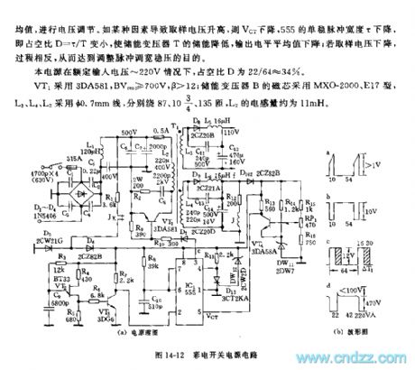
As the figure 14-12 shows, the color TV switching power supply uses the pulse width modulation mode, the pulse width adjustment range is wide, and the voltage stabilizing effect is good, when the input voltage is in the range of 12 to 280V, the output DC voltage is +110V+/-1V.
The double-base port transistor relaxation oscillator is composed of the VT2 and R3, R5, C9, it is used as the time base pulse source, and it is amplified by the VT3 that can be used as the trigger pulse of IC1(555). The controllable monostable trigger circuit is composed of the 555 and the R8, C10. The temporary stability time depends not only on the R8 and the charging time constant of C10, but also the sampling voltage VCT. By changing the duty ratio of the 555's output pulse, you can change the voltage. The output square wave of 555 adds to the power amplifier tube VT1 to encourage the switching power supply of the collector load.
(View)
View full Circuit Diagram | Comments | Reading(1279)
The 555 touch audio circuit
Published:2011/6/16 2:18:00 Author:TaoXi | Keyword: 555, touch audio
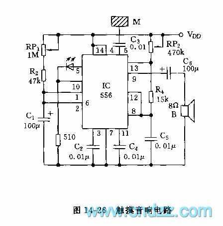
As the figure 14-26 shows, the monostable trigger and the multivibrator are composed of a double-time base 556 and some RC components. When the hand touches the sheetmetal M, the induction signal of human body adds to the trigger port pin-6 of IC through C3, so the circuit is triggered, the output port pin-5 of this time base circuit is from the low level to the high level. Because the astable multivibrator's time base circuit reset port pin-10 has the high electrical level, so the oscillator starts working, the oscillation frequency is between 300~4500Hz, so the speaker sends out the sound. When the monostable circuit is triggered, the power supply voltage charges to C1 through RP1 and R2, the delay time td=1.1(RP1+R2)C1.
(View)
View full Circuit Diagram | Comments | Reading(539)
555 touch mode 10 stages volume automatic regulator circuit
Published:2011/6/16 2:01:00 Author:TaoXi | Keyword: 555, touch mode, 10 stages, volume, automatic regulator
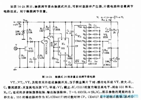
As the figure 14-24 shows, the touch regulator is composed of the touch switch, the controllable time base pulse generator, the counting circuit and the volume control circuit, this touch regulator can be used to touching control the volume.
The touch switch is composed of the VT1, VT2, VT3 and the resistance capacitance components. When the hand touches the sheetmetal T, the induced voltage is amplified by VT1, then it is rectified and filted by D1 and C1, the DC voltage conducts the VT2, and the VT3 cuts off, the reset port of IC1(555) has the high electrical level, the multivibrator which is composed of the 555 and R7,R8,C2 starts working to output the oscillation pulse. T=0.693(R7+2R8)C2, the cycle of the figure parameter is about 3 seconds. The output pulse of 555 can be used as the count clock CP of the IC2(CD4017). The CD4017 is the decimal counter / pulse distributor.
(View)
View full Circuit Diagram | Comments | Reading(1164)
| Pages:1648/2234 At 2016411642164316441645164616471648164916501651165216531654165516561657165816591660Under 20 |
Circuit Categories
power supply circuit
Amplifier Circuit
Basic Circuit
LED and Light Circuit
Sensor Circuit
Signal Processing
Electrical Equipment Circuit
Control Circuit
Remote Control Circuit
A/D-D/A Converter Circuit
Audio Circuit
Measuring and Test Circuit
Communication Circuit
Computer-Related Circuit
555 Circuit
Automotive Circuit
Repairing Circuit