
Signal Processing
Index 158
The zero passage circuit (experiment approved)
Published:2011/6/28 0:41:00 Author:Borg | Keyword: zero passage
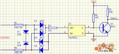
View full Circuit Diagram | Comments | Reading(538)
555 sound and light simultaneous display stress electronic metronome circuit
Published:2011/6/15 9:52:00 Author:TaoXi | Keyword: 555, sound, light, simultaneous display, stress, electronic metronome
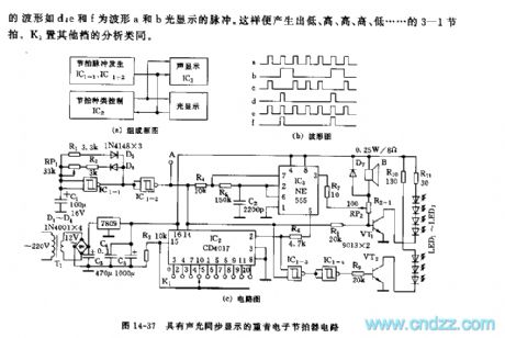
The stress electronic metronome is composed of the beat pulse generator, the beat type controller and the sound & light circuit, as the figure 14-37(a) shows, figure (b) is the waveform of all levels, figure (c) is the circuit. This metronome has 1-10 ten kinds of beat ways, the beat speed is 40-208 times/minute.
The IC1-1(1/4CD4093) quad 2 input Schmitt trigger is connected as the beat pulse oscillator, the positive pulse width is 100ms, RP1 can be used to change the pulse interval. The IC2(CD4017) is the 1-10 circulation counter, the cycling time is set by K1. In this figure, K1 is in the position of 4 , the waveform b is the output pulse of it. The IC3(555) is under the action of the waveforms a and b to output the high tone sound waveform such as c.
(View)
View full Circuit Diagram | Comments | Reading(1129)
555 ten notes continuous playing circuit
Published:2011/6/15 8:11:00 Author:TaoXi | Keyword: 555, ten notes, continuous playing
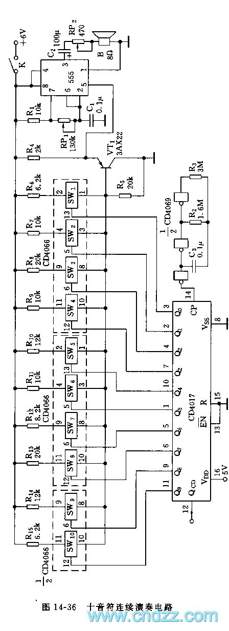
As the figure 14-36 shows,the frequency controllable multivibrator is composed of the 555 time-base circuit and some capacitance resistance components. The control port pin-5 of 555 is connected with the output port of the launch follower VT1, and the VT1 is controlled by the time sequence switching circuit to make the 555 to produce the ten notes of 6 1 3 1 2 1 7 3 2 6.
The oscillator which has the period of 0.6s is composed of the CMOS six phase-inverter CD4069 and three gate circuits, the notes add to the time sequence distributor which is composed of the decimal counter CD4017 to make the 10 output ports of it controls the four two-way switch circuit CD4066 respectively, and these switches turn on one by one and it adds to the base electrode of the emitter-follower VT1.
(View)
View full Circuit Diagram | Comments | Reading(458)
Digital preset circuit and the 128 buttons keypad scanning circuit
Published:2011/6/20 0:50:00 Author:TaoXi | Keyword: Digital preset, 128 buttons, keypad scanning


The digital preset circuit
The function of this circuit: it changes the keyboard pressing signal into the 2-bit BCD code and stores the code. Figure 1 is the logic diagram of this coding and storage circuit.
Keypad scanning circuit
In the last example, the keyboard scale is small, it has only ten keys (0-9). If the keyboard scale is large, by using the priority encoders to realize the coding will not economic any more. So people design the keypad scanning circuit. Figure shows the 128 keys scanning encoder.
(View)
View full Circuit Diagram | Comments | Reading(2872)
acousto-optic logical pen circuit of NE555
Published:2011/6/17 6:44:00 Author:chopper | Keyword: acousto-optic, logical pen,

View full Circuit Diagram | Comments | Reading(580)
Triangle wave and sine wave producing circuit
Published:2011/6/20 3:09:00 Author:TaoXi | Keyword: Triangle wave, sine wave, producing circuit
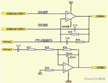
The input signal of the triangle wave producing circuit is from the EPWM1A's pin of the DSP, this signal is the PWM signal, it is integrated and changes into the triangle wave, then it is sent into the PWM producing circuit. The PWM signal which comes fron the TMS320F28335 is filtered by the second stage low-pass to produce the sine wave reference signal, this signal inverts with the inverter output voltage feedback signal. The PWM signal which is output by the pin of the EPWM2A is the city electricity input tracking signal, this circuit has the regulation function to the input sine wave signal. The figure shows the triangle wave and sine wave producing circuit.
(View)
View full Circuit Diagram | Comments | Reading(880)
TA1343N surround processing integrated circuit
Published:2011/6/16 1:17:00 Author:chopper | Keyword: surround processing, integrated circuit
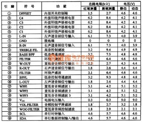
TA1343N is a surround processing integrated circuit produced by Company TOSHIBA,and it is applied to homemade and import large-screen color TV,such as Haier large-screen color TV and so on.TA1343N integrated circuit adopts dual inline 24 pinned package,and it is applied to Body strong 34F9B-TD large-screen color TV of Haier.Its function and data of integrated circuitare shown as chart 1. (View)
View full Circuit Diagram | Comments | Reading(834)
(CD4011) vocal type logical pen circuit of gate circuit
Published:2011/6/22 9:41:00 Author:chopper | Keyword: vocal type, logical pen, gate circuit

View full Circuit Diagram | Comments | Reading(629)
(CD4069) message display type logical pen circuit of gate circuit
Published:2011/6/22 9:44:00 Author:chopper | Keyword: message display type, logical pen, gate circuit

View full Circuit Diagram | Comments | Reading(574)
(CD4011) message display type logical pen circuit of gate circuit
Published:2011/6/22 9:58:00 Author:chopper | Keyword: message display type, logical pen circuit, gate circuit

View full Circuit Diagram | Comments | Reading(635)
(CD4069) message display logical pen circuit of gate circuit
Published:2011/6/20 6:42:00 Author:chopper | Keyword: message display, logical pen, gate circuit

View full Circuit Diagram | Comments | Reading(639)
(CD4001)message display logical pen circuit of gate circuit
Published:2011/6/17 20:38:00 Author:chopper | Keyword: message display, logical pen, gate circuit

View full Circuit Diagram | Comments | Reading(628)
(CD4001) logical pen circuit with function of displaying the open circuit
Published:2011/6/17 6:53:00 Author:chopper | Keyword: logical pen, display the open circuit

View full Circuit Diagram | Comments | Reading(657)
logical pen of Luminous display type circuit of NE555
Published:2011/6/17 6:46:00 Author:chopper | Keyword: Luminous display, logical pen circuit

View full Circuit Diagram | Comments | Reading(564)
Voltage Control Function Generator Circuit of μA709
Published:2011/6/25 21:45:00 Author:Michel | Keyword: Voltage Control, Function Generator, Circuit

The picture 6-50 is the voltage control function generator circuit of μA709.In the circuit,A1 is charge reversal circuit,VT1~VT4 are analog switches,A2 is mueller integral circui,A3 and A4 are PWL comparing circuit,VT6,VT5 and G1-G3 are trigger circuit.VT1 and VT2 analog switches control voltgae UT to control the operational amplifier A1, integrating circuit's intergration composed of timing resistance RT (RT1 and RT2) and the forms of A2 output linear rising and fall.If VT1 conducts,A2 output linear declines because positive step voltgae intergrates. (View)
View full Circuit Diagram | Comments | Reading(2018)
The AD108 frequency doubler allowing asymmetric square wave input
Published:2011/6/17 8:23:00 Author:Borg | Keyword: frequency doubler, asymmetric square wave
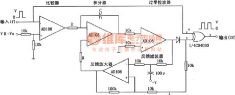
In the figure is the frequency doubler allowing asymmetric square wave input. This circuit characterizes wide frequency range, and it is not affected by the power supply voltage change, it also receives asymmetric input signals. When the input is a square wave, the input signal is turned into a dual polarity wave by a high gain comparator and then added on an integrator. The input of the integrator is the triangular wave. The wave crosses the zero line at T/4 and 3T/4(T is the period of the input signal), after the triangular wave has been sent to the zero detector, the 90⁰ lagged phase square wave is generated. (View)
View full Circuit Diagram | Comments | Reading(1125)
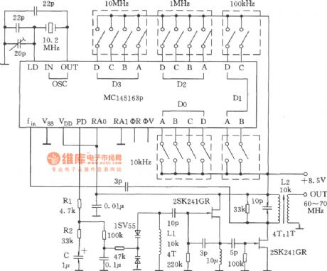
The 60~70MHz PLL frequency synthesizer circuit composed of MC145163P
Published:2011/6/17 6:55:00 Author:Borg | Keyword: frequency synthesizer, PLL
View full Circuit Diagram | Comments | Reading(3093)
The odd-even frequency splitter composed of SN74193
Published:2011/6/17 22:14:00 Author:Borg | Keyword: frequency splitter
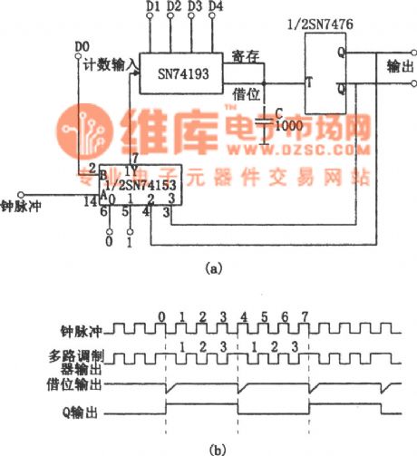
In the figure is the odd-even frequency splitter circuit. This circuit can engage in 2~32 (including odd and even) times of splitting. The counting input of the synchronized counter SN74193 is provided by the output 1Y of the multiplexer SN74153, the borrow output of the counter can not only drive the trigger SN7476, but also it's the deposit input pulse of SN74193. The 5-bit binary numbers are imposed on D0, D1, D3 and D4 input terminals, which decides the splitting constant(2~32), and D0 is the lowest bit. When D0=0, the outputting pulse phase of the multiplexer is determined according to the trigger state. (View)
View full Circuit Diagram | Comments | Reading(1241)
The digital frequency doubler(LM108 and LM111)
Published:2011/6/17 9:45:00 Author:Borg | Keyword: digital frequency doubler
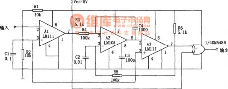
The circuit consists of the voltage comparator, Miller integrator and OR gate. A1 is the LEV comparator, which is fulfilled by the chip LM111, the chip forms the rectifier circuit that converts the long-rising-time waveform (such as the sine wave) to the short-rising-time square wave. The square wave output by A1 is turned into the triangular wave by the Miller integrator which consists of A2, R4 and C4, and then the LEV comparator A3 turns the triangular wave into the square wave. There is a 90⁰ phase difference between A1 and A3, so after crossing the the OR gate, the wave is doubled and then output. (View)
View full Circuit Diagram | Comments | Reading(655)
The frequency splitter of symmetric output waveforms (μL9020)
Published:2011/6/22 4:29:00 Author:Borg | Keyword: frequency splitter, symmetric output waveforms
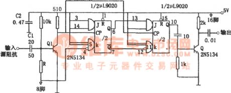
The figured splitter circuit is triggered when the peak value is in the range of 0.5~5v, no matter whether it is the sine wave or the square wave. The working frequency of the circuit is 40MHz. The input signal of the frequency splitter drives the J-K triggers after it has passed the amplitude limit amplifier Q1, finally, it crosses the buffer Q2 and is output. The transistor Q1 offers the first stage splitter a proper triggering LEV. When the high LEV drives, the capacitor C1 plays a part of current limitation. If the drive LEV is low, we can expand the volume of C1, the the trigger power is increased. (View)
View full Circuit Diagram | Comments | Reading(527)
| Pages:158/195 At 20141142143144145146147148149150151152153154155156157158159160Under 20 |
Circuit Categories
power supply circuit
Amplifier Circuit
Basic Circuit
LED and Light Circuit
Sensor Circuit
Signal Processing
Electrical Equipment Circuit
Control Circuit
Remote Control Circuit
A/D-D/A Converter Circuit
Audio Circuit
Measuring and Test Circuit
Communication Circuit
Computer-Related Circuit
555 Circuit
Automotive Circuit
Repairing Circuit