
Signal Processing
Index 155
Unijunction transistor sawtooth wave generator circuit
Published:2011/7/4 19:34:00 Author:Christina | Keyword: Unijunction transistor, sawtooth wave, generator circuit
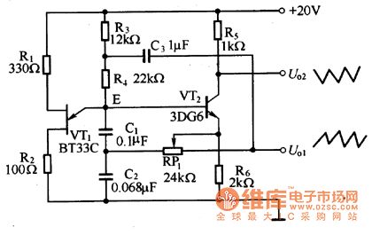
The sawtooth wave generator circuit is as shown in figure 1. It uses the unijunction transistor multivibrator as the foundation, and it has a emitter follower. It can produce the positive and negative sawtooth wave voltage which has good linearity.
Figure 1 The sawtooth wave generator circuit principle diagram
(View)
View full Circuit Diagram | Comments | Reading(1460)
27MHz quartz crystal oscillator circuit
Published:2011/7/4 6:27:00 Author:Christina | Keyword: 27MHz, quartz crystal, oscillator circuit

The 27MHz quartz crystal oscillator circuit is as shown in figure 1. The biasing circuit is composed of the R1, R2 and R3, C6 is the bypass capacitor. The partial voltage circuit is composed of the C1, C2, C3 and C4 to control the strength of oscillation. L1 is the high-frequency choke coil, it has the role of filtering.
Figure 1 The 27MHz quartz crystal oscillator circuit
The quartz crystal resonator JAl2B is in the parallel resonant state, the oscillation frequency of the oscillator depends on the natural frequency of the crystal. The L2 and C5 determine the oscillation strength. (View)
View full Circuit Diagram | Comments | Reading(3419)
44MHz quartz crystal oscillator circuit
Published:2011/7/4 6:20:00 Author:Christina | Keyword: 44MHz, quartz crystal, oscillator
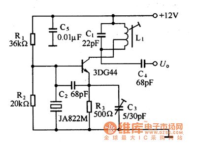
The 44MHz quartz crystal oscillator circuit is as shown in figure 1. In order to get the high oscillation frequency, this circuit uses the frequency multiplication oscillation circuit. The L1 and C1 tune at 44MHz, the fundamental wave 22MHz is mistermination, so this is the short-circuit. The quartz crystal resonator uses the 22MHz resonator, it has the sensibility in the circuit, the partial voltage capacitance are C2 and C3. For the 22MHZ fundamental wave, the circuit is the three-point capacitance oscillation circuit, you can get the 22MHz oscillation signal from the emitter.
Figure 1 The 44MHz quartz crystal oscillator circuit
(View)
View full Circuit Diagram | Comments | Reading(749)
100MHz quartz crystal oscillator circuit
Published:2011/7/4 6:12:00 Author:Christina | Keyword: 100MHz, quartz crystal, oscillator
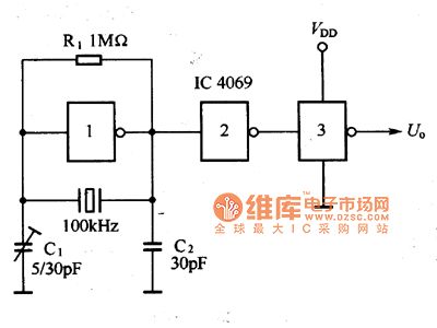
The high precision frequency oscillator circuit which is composed of the 100kHz quartz crystal resonator and the phase inverter is as shown in the figure 1, the phase inverter 2 and phase inverter 3 are the shaping circuit.
Figure 1 The 100kHz quartz crystal oscillator circuit
(View)
View full Circuit Diagram | Comments | Reading(3022)
1MHz quartz crystal oscillator circuit
Published:2011/7/4 6:08:00 Author:Christina | Keyword: 1MHz, quartz crystal, oscillator

The oscillator circuit which is composed of the 1MHz quartz crystal resonator and the NAND gate is as shown in the figure, the NAND gate 3 is the output buffer stage. This circuit can be used to calibrate the standard frequency.
Figure 1 The 1MHz quartz crystal oscillator circuit
(View)
View full Circuit Diagram | Comments | Reading(2475)
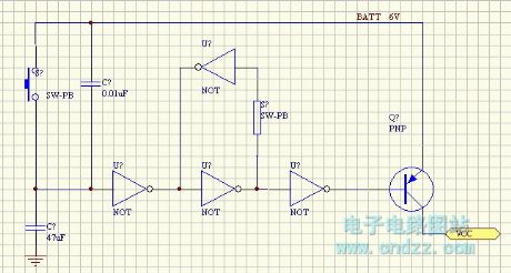
The key waking circuit
Published:2011/7/4 4:30:00 Author:Seven | Keyword: key waking
View full Circuit Diagram | Comments | Reading(743)
465kHz amplitude modulation intermediate frequency signal generator circuit
Published:2011/7/4 1:54:00 Author:Christina | Keyword: 465kHz, amplitude modulation, intermediate frequency, signal generator

The 465kHz amplitude modulation intermediate frequency signal generator circuit is as shown in the figure 1. The 400Hz low-frequency multivibrator is composed of the VT1 and VT2, the 465kHz intermediate frequency oscillator is composed of the VT3, VT4 and the ceramic filter 3L465. The 400Hz low-frequency modulates the 465KHZ intermediate frequency signal through C3, and the modulated 465kHz intermediate frequency signal is output by the emitter VT4. The ceramic filter of the circuit has the frequency selection function. The potentiometer RP can be used to adjust the output amplitude.
Figure 1 The 465kHz amplitude modulation intermediate frequency signal generator circuit
(View)
View full Circuit Diagram | Comments | Reading(2832)
The HCS301 encoder application circuit in wireless emitting circuits
Published:2011/7/3 22:23:00 Author:Borg | Keyword: encoder, wireless emitting circuits
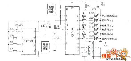
HCS301 rolling encoder chip is developed on the base of non-linear flow code algorithm, which includes the 66-bit transmitting code, 32-bit rolling code, 64-bit programmable secrete key, 32-bit source code, which can generates 266 kinds of combination, which can make sure that the codes won't repeat in 18 years. The special algorithm can make the rolling decoder only react to a code once in the valid period, and every code is sent randomly, the decoding is impossible. The HCS301 encoder circuit, which is applied in wireless emitting circuits, is shown in the figure.
(View)
View full Circuit Diagram | Comments | Reading(4342)
(CD4069) shine type logical pen circuti of gate circuit
Published:2011/6/20 6:39:00 Author:chopper | Keyword: shine type, logical pen, gate circuit

View full Circuit Diagram | Comments | Reading(621)
The infrared monitor wireless alarm circuit
Published:2011/7/1 22:17:00 Author:Borg | Keyword: infrared monitor, wireless alarm
In the figure is the infrared monitor wireless alarm circuit. The circuit consists of the infrared monitoring emitter and the infrared reception circuit, two parts in total, which are shown in figure (a) and figure (b) respectively. Figure (a) adopts two CMOS 555 chips (or one 556), IC1 and IC2, the two outputs the waveforms of 1.5KHz and 35KHz respectively, of which the 1.5KHz square wave is used to modulate the loading wave. In the figure, IC1 is connected as a multi-resonance oscillator, whose oscillating frequency is 1.5KHz, and the corresponding charge/discharge time is decided by the time constant. The duty cycle of the square wave output by IC1 is 1:3 (160μs:500μs).
(View)
View full Circuit Diagram | Comments | Reading(628)
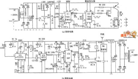
The rolling code encoding wireless emitting circuit(HSC360/TDA5100)
Published:2011/7/1 21:30:00 Author:Borg | Keyword: rolling code, wireless emitting circuit
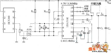
Figure:The rolling code encoding wireless emitting circuit(HSC360/TDA5100)TDA5100 is a ultra-high frequency wireless emitting circuit produced by Seimens, whose internal structure is complex, function is full, sensibility is high, output signal amplitude is high, external elements are few and price is low, it is a excellent emitting circuit. (View)
View full Circuit Diagram | Comments | Reading(1232)
The infrared burglarproof alarm circuit
Published:2011/7/1 22:51:00 Author:Borg | Keyword: infrared, burglarproof alarm
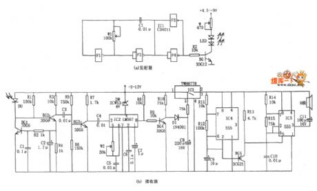
In the figure is the infrared burglarproof alarm circuit. The alarm includes the infrared pulse emitter and receiver, the decoder and alarm stereo circuit, and the emitter and receiver are installed on the same metal base. The emitter is a multi-resonance oscillator composed of 4 NAND CD4011 with two input terminals, whose oscillating frequency is decided by W1 and C1, the frequency corresponding to the figured parameters is about 1~15kHzm, the oscillating signal is turned into the infrared pulse signal after it is driven by BG. The infrared receiver and decoder includes the infrared light-electricity converter and so on.
(View)
View full Circuit Diagram | Comments | Reading(620)
The infrared sound/light alarm circuit
Published:2011/7/1 23:23:00 Author:Borg | Keyword: infrared, sound/light alarm
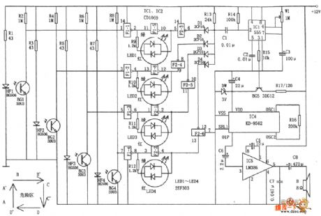
In the figure is the infrared sound/light alarm circuit.The circuit consists of the AND gate circuit, single steady time delay circuit, 4 lines of infrared emitter and the reception circuit, trigger and 2-color light circuit, stereo alarm circuit and so on. The alarm is used in alarm area, and the range is shown in the figure. The infrared LED HF1~HF4 and the coupling pipes BG1~BG4(3DU31) compose 4 pairs of emitting and receiving warning lines.If someone is passing the warning line, the infrared ray is blocked, so the corresponding coupling pipe is blocked and the NAND inputting a high LEV.
(View)
View full Circuit Diagram | Comments | Reading(1170)
The circuit design reference diagram
Published:2011/7/1 23:54:00 Author:Borg | Keyword: circuit design, reference diagram
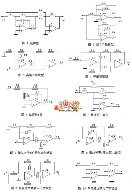
The precise full-wave rectifier circuit in the figure is named by myself, which is only for distinguishing; unless there are special instructions, or the gains are all designed according to 1. In figure 1 is the most classical circuit, whose virtue is that it can connect with a filter capacitor in the parallel way on R5. The coupling relation is R1=R2, R4=R5=2R3. It can also adjust the gain by changing R5. The circuit in figure 2 characterizes few resistors, which only requires R1=R2. The circuit in figure 3 characterizes high input impedance, the coupled resistor requires R1=R2, R4=2R3. All the coupled resistors in figure 4 are the same, and the gain can be adjusted by changing R1.
(View)
View full Circuit Diagram | Comments | Reading(562)
down-lead of high frequency circuit
Published:2011/6/27 9:30:00 Author:chopper | Keyword: down-lead, high frequency circuit
In the high frequency circuit,the inductance and capacitance of the down-lead effect circuit a lot and the supply lead is very important.We should reduce the impedance of landlines as possible as we can in the high frequency range.As for high frequency circuit, it includes landlines basically besides element lines and signal lines.Thus,all parts of the groud of the circuit can be connected by any routes and the impedance among the groud is very low.The picture a,b are printed plate wiring examples of single pipe broadband amplifier circuit.We can know there are all landlines besides down-leads.
(View)
View full Circuit Diagram | Comments | Reading(496)
one point connetion method of amplification circuit
Published:2011/6/27 22:15:00 Author:chopper | Keyword: one point connetion method, circuit

Thus,it needs one point connetion method.The so-called one point connetion means the reference potentials of every part are the same.The picture a,b is the one point connetion method.As the picture (a),the ground of input end and amplifier is connected to the ground of power supply by one line.Therefore,all return current is circulated between the input signal ground and the amplifier.If among the benchmark ground there is a wiring resistor RC,it will generate noise and hum.
(View)
View full Circuit Diagram | Comments | Reading(604)
landlines of low frequency circuit
Published:2011/6/27 21:59:00 Author:chopper | Keyword: landlines, low frequency circuit

In the low frequency circuit,different grounding methods will effect a lot to the circuit performance when deal with the weak level signal.The picture a,b are the grounding methods of amplifier circuit.The picture (a) is a inverse amplification circuit,and it takes the same phase input terminal of operational amplifier as benchmark by connecting it to ground through resistor to amplify.The picture(b) is a in phase amplification circuit and it takes the inverse input end of operational amplifier as benchmark by connecting it to ground through resistor to amplify.
(View)
View full Circuit Diagram | Comments | Reading(582)
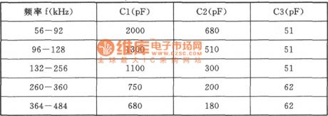
56~484 High Frequency Oscillator Circuit
Published:2011/6/21 3:54:00 Author:Joyce | Keyword: 56~484, High Frequency , Oscillator
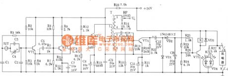
As shown in the figure is a high frequency oscillator, which can be used as an exclusive high frequency generator. Different values of capacitance will produce a high frequency sine wave in the range between 56 to 484 kHz. This circuit has the characteristics of good waveform, high frequency stability, and low output impedance and so on.
Choice of components:
Transistor VT1, VT2: 3 DG6D, 65≤β≤115, VT3、 VT4:3 DG 1308, 60≤β≤85. Semi-adjustable capacitors C4: CCWX-3-5/20 pF. Quartz crystal SJT: BE-42. K: JZX-10 M (miniature relay). Light emitting diode VD4: BT-605 (red, green). Transformer T: MXD-2000 ferrite, GV- 30x 19magnetic core.DLL-2. Φ 0.21 mm high strength enameled wire, rolled in 133 turns, L3-4 Φ0.21 mm high strength enameled wire rolled in 11 turns , L5-6 Φ0.21 mm high strength enameled wire, rolled in 80 turns. Except resistance R27 which adopts l/2WRJ , all the other resistance use 1/8 WRJ.
The relationship between the frequency and capacitance values are shown in the following figure.
(View)
View full Circuit Diagram | Comments | Reading(613)
Collpitts Oscillator Circuit
Published:2011/6/21 3:33:00 Author:Joyce | Keyword: Collpitts , Oscillator
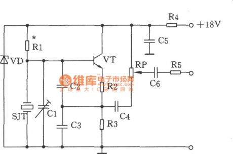
As shown in the figure is a colpitz oscillator circuit. It has a crystal with fundamental frequency of 1499 kHz. Crystal SJT is connected at the ends of capacitance C2 and C3 in parallel. Emitter divider resistances R2, R3 will provide basic feedback signals, which are controlled by capacitance dividers C2 and C3. After crystal SJT starts oscillation, it will transfer sine signals of 1499 kHz to audion VT base, and the signals will be output through emitter follower VT. Then they will go through coupling capacitance C4 to potentiometer RP. Resistance R1 would give a suitable offset voltage to VT by depressing the 18 V voltage. (View)
View full Circuit Diagram | Comments | Reading(602)
The South-east Wagon central control and warning equipment system circuit
Published:2011/6/30 20:53:00 Author:qqtang | Keyword: central control, warning equipment system
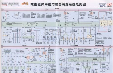
The South-east Wagon central control and warning equipment system circuit is shown as above.
(View)
View full Circuit Diagram | Comments | Reading(481)
| Pages:155/195 At 20141142143144145146147148149150151152153154155156157158159160Under 20 |
Circuit Categories
power supply circuit
Amplifier Circuit
Basic Circuit
LED and Light Circuit
Sensor Circuit
Signal Processing
Electrical Equipment Circuit
Control Circuit
Remote Control Circuit
A/D-D/A Converter Circuit
Audio Circuit
Measuring and Test Circuit
Communication Circuit
Computer-Related Circuit
555 Circuit
Automotive Circuit
Repairing Circuit