
Signal Processing
Index 157
Low frequency Therapeutic Equipment (the 3rd)
Published:2011/6/28 7:50:00 Author:Felicity | Keyword: Low frequency Therapeutic Equipment (the 3rd)
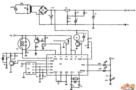
Work of the circuit
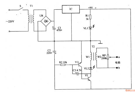
The circuit consists of power circuit IC and pulse pressure producing circuit. (It is showed in picture 9-21.)
Turn on the power switch. The 220V AC voltage is adjusted. It then separates into two parts. One supplies 9V DC voltage to the pulse pressure producing circuit. And the other is limited by R1 and lightens VL1.
The low frequency OSC works and VL2 shines. And winding W2 of T2 produces pulse pressure. The pressure is adjusted by RP and added to the acupoints. It gives some assisting treatment to some chronic diseases. (View)
View full Circuit Diagram | Comments | Reading(779)
Low frequency Therapeutic Equipment (the 2nd)
Published:2011/6/28 7:51:00 Author:Felicity | Keyword: Low frequency Therapeutic Equipment (the 2nd)
Work of the circuit
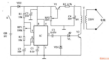
The circuit consists of time based integrated circuit IC, transistor V1, V2 and pulse transformer T. (It is showed in picture 9-20.)
Turn on the power switch S and the OSC begins to work. Pin 3 of IC produces pulse signal of low frequency. This signal makes V2 working. Then the pressure is transmitted to muscular tissue or acupoints. It relaxes or stimulates acupoints to give some assisting treatment to some chronic diseases.
(View)
View full Circuit Diagram | Comments | Reading(1147)
Low frequency Therapeutic Equipment (the 1st)
Published:2011/6/28 7:53:00 Author:Felicity | Keyword: Low frequency Therapeutic Equipment (the 1st)
Work of the circuit
The circuit consists of RC OSC, buffer amplifying circuit and outputting circuit. (It is showed in picture 9-19.)
RC produces oscillating pulse. The pulse is amplified by V2 and V3. It is also stepped up by T. Then it produces pulse voltage of low frequency on the winding W3 of T. The voltage is adjusted by RP. It is added to the patient’s acupoint though two poles of XS. It stimulates body’s main and collateral channels to treat illness.
(View)
View full Circuit Diagram | Comments | Reading(438)
Ultrasonic Therapeutic Equipment (the 2nd)
Published:2011/6/28 7:55:00 Author:Felicity | Keyword: Ultrasonic Therapeutic Equipment (the 2nd)
Work of the circuit
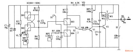
The circuit consists of power circuit, timer, controlling circuit, outputting circuit and ultrasonic vibration. (It showed in picture 9-17.)
Turn on power switch S3. 15V voltage of GB separates into two parts. One is supplied to the ultrasonic vibration. And the other one is adjusted and produces 10V DC voltage. The DC voltage works as IC’s working voltage. And it is limited by R3 and lightens VL1.
When the ultrasonic vibration is working, pulse voltage of high frequency. The pulse voltage glow discharges human body through HL.
Put S2 in the position “1”, the ultrasonic vibration is influenced by timer. Press S1 and the ultrasonic vibration works without pause. When the regular time is over, the ultrasonic vibration outputs discontinuous ultrasonic. (View)
View full Circuit Diagram | Comments | Reading(564)
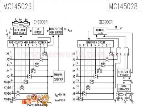
The MC145028 circuit
Published:2011/6/29 5:22:00 Author:Seven | Keyword: circuit
View full Circuit Diagram | Comments | Reading(764)
The 10-line chasing type flash circuit
Published:2011/6/29 5:46:00 Author:Seven | Keyword: chasing type
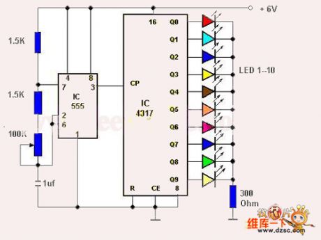
View full Circuit Diagram | Comments | Reading(463)
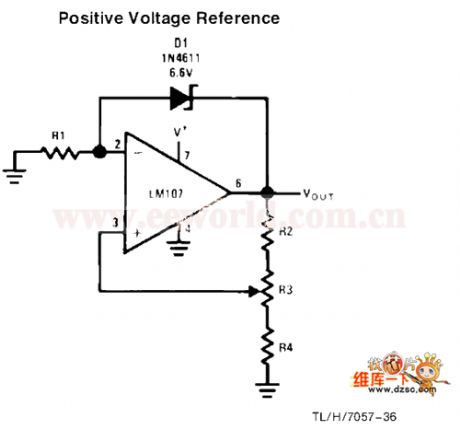
The positive voltage reference circuit
Published:2011/6/29 6:15:00 Author:Seven | Keyword: positive, voltage reference
View full Circuit Diagram | Comments | Reading(569)
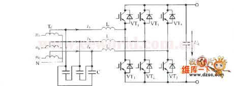
The 3-phase PWM rectifier sturcture circuit
Published:2011/6/29 6:20:00 Author:Seven | Keyword: 3-phase, PWM rectifier, sturcture circuit
View full Circuit Diagram | Comments | Reading(1410)
The water sound sensor application circuit
Published:2011/6/29 6:48:00 Author:Seven | Keyword: water sound sensor, application circuit
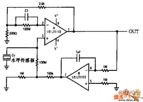
The water sound sensor application circuit is shown as above.
(View)
View full Circuit Diagram | Comments | Reading(1033)
The carbon monoxide sensor circuit
Published:2011/6/29 20:54:00 Author:Seven | Keyword: carbon monoxide, sensor
The carbon monoxide sensor circuit is shown as above.
(View)
View full Circuit Diagram | Comments | Reading(4188)
The inductance oscillator circuit of 3-point type
Published:2011/6/29 21:09:00 Author:Seven | Keyword: inductance, oscillator circuit
The inductance oscillator circuit of 3- point type is shown in the figure.
(View)
View full Circuit Diagram | Comments | Reading(646)
Infrared remote control 40Hz carrier wave signal generating circuit
Published:2011/6/26 5:51:00 Author:TaoXi | Keyword: Infrared remote control, 40Hz, carrier wave, signal generating circuit
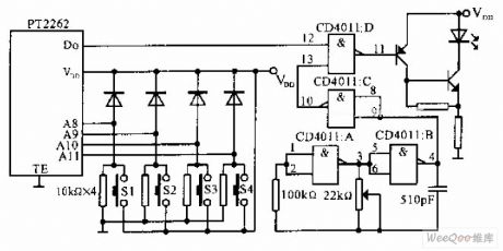
The circuit that uses the infrared remote control 40Hz carrier wave signal generating circuit as the infrared transmitter is as shown in the figure, when you press one or several buttons of the S1-S4, the PT2262 gets power to work and it outputs the pulse data flow. At the same time, the pulse oscillator which is composed of the CD4011 and CD4011B starts working, the oscillation frequency can be adjusted to 40KHz by the 22Ω potentiometer, the frequency is the infrared carrier wave frequency. The output data flow of PT2262 modulates the 40KHz carrier wave in the CD4011D, then the output data flow drives the infrared led through the transistor to output the infrared signal.
(View)
View full Circuit Diagram | Comments | Reading(1235)
Voltage control oscillator circuit composed of the Schmitt trigger
Published:2011/6/26 3:08:00 Author:TaoXi | Keyword: Voltage control oscillator, Schmitt trigger
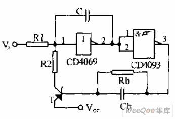
The voltage control oscillator (negative voltage control oscillator) that is composed of the Schmitt trigger is as shown in the figure, the oscillation frequency decreases with the increasing of VA, the variation range of VA is VSS-VTBC, this kind of circuit has wide adjustment range and good linear relation.
(View)
View full Circuit Diagram | Comments | Reading(663)
555 simple electronic keyboard circuit (2)
Published:2011/6/15 19:24:00 Author:TaoXi | Keyword: 555, simple, electronic keyboard

As the figure 14-41 shows, the multivibrator is composed of the 555 and some capacitance resistance components, the oscillation frequency depends on the values of Ra, R16 and C3. f=1.44/(Ra+2R16)C3, the Ra of the formula corresponds to the different values of R1-R15, this depends on the situation of the keys K1-K15. When you are debugging the notes, you can use a 100kΩ potentiometer to debug repeatedly, and confirm every note's corresponding resistance. This circuit uses the bipolar type 555, this 555 can drive the speaker directly.
(View)
View full Circuit Diagram | Comments | Reading(1439)
The multi-waveform generator of good functions
Published:2011/6/14 21:31:00 Author:Borg | Keyword: multi-waveform generator, good functions
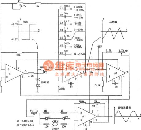
In the figure is the multi-waveform generating circuit of good functions. This circuit is fixed with 4 high impedance computing amplifiers, which can generates low-frequency, ultra-low-frequency, triangular and sine wave. In the figure, A1 functions as the voltage rectifier, A2 forms the integrator, the integration capacitor is selected by the switch. A1 and A2 are connected in a loop, which compose a typical triangular and square oscillator. The output stable pipe of A1 is used to stabilize the amplitude of the square wave, and it also increases the stability of the whole circuit. (View)
View full Circuit Diagram | Comments | Reading(518)
The odd frequency divider counter of the symmetric output waveform(SN7474 and SN74163)
Published:2011/6/26 20:25:00 Author:Borg | Keyword: frequency divider, symmetric output waveform
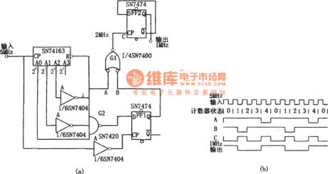
In the figure is the odd frequency divider counter of the symmetric output waveform(SN7474 and SN74163). Sometimes, we need to divide the clock pulse at odd times, and the duty cycle is 50%. Under this condition, an ordinary counter just needs 2 triggers and several gate circuits, see as the figure. When the 20-bit of the counter is logic 1 , meanwhile,21 and 22-bit output 0 logic, the B point is logic 0 ; when the 22-bit of the counter is 1 , the logic of A is 0 . (View)
View full Circuit Diagram | Comments | Reading(1754)
The frequency divider (CD4040) of converting the 50Hz or 60Hz into their 1/60
Published:2011/6/26 20:15:00 Author:Borg | Keyword: frequency divider, 50Hz, 60Hz
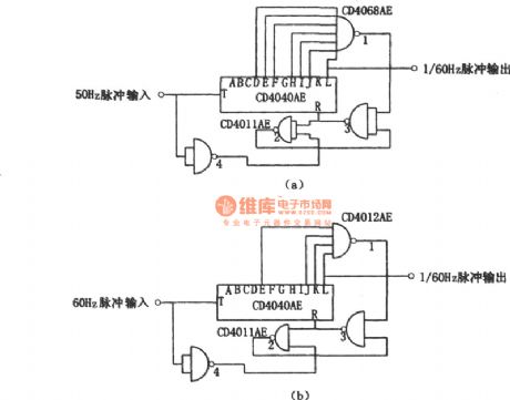
In the figure is the frequency divider (CD4040) of converting the 50Hz or 60Hz into their 1/60. As CMOS is integrated, and it's multi-stage, so a CMOS integrated circuit can divede the 50Hz or 60Hz signals, and they are output at the period of 1min. This circuit is installed with a 12-stage counter CD4040AE, which can switch the 50Hz input pulse signal into the output pulse whose period is 1min, the dividing coefficient is 50×60=3000. The way to change the decimal 3000 into to binary is to divide 3000 by 2 continuously, all the even number is marked as 0 .
(View)
View full Circuit Diagram | Comments | Reading(3195)
The digital frequency divider (SN7490, SN7442 and SN74150)
Published:2011/6/26 20:35:00 Author:Borg | Keyword: digital frequency divider
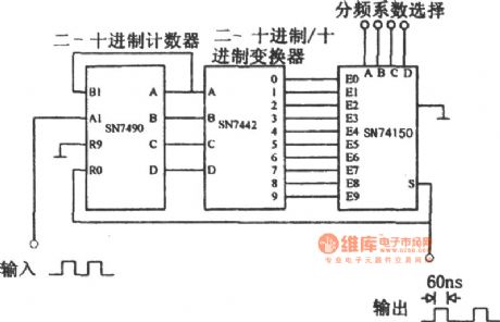
In the figure is the digital frequency divider, which consists of 3 integrated circuits, and its dividing coefficient ranges from 1 to 9. The counter SN7490 outputs the binary-coded decimal numbers which are sent to the decoder SN7442, and the decoder outputs decimal numbers. The dividing coefficient is decided by the selector SN 74150. The output of the data selector is fed back to the reset input terminal of SN7490, i.e a pulse is output once a counting period is over, the pulse is resetting the counter SN7490 at the same time. The width of the pulse is 60ns, which is decided by the delayed transmitting time. (View)
View full Circuit Diagram | Comments | Reading(3517)
The 555 pulse electric therapeutic apparatus circuit
Published:2011/6/27 22:11:00 Author:Borg | Keyword: pulse, electric therapeutic apparatus
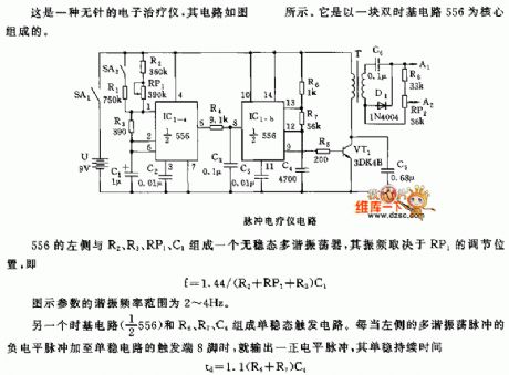
This is the stingless electric therapeutic apparatus, whose circuit is shown in the figure. It is formed based on a dual time-based circuit 556.
The pulse electric therapeutic apparatus circuit The left side of 555 composes an astable multi-resonance oscillator with R2, R3, RP1 and C1, whose oscillating frequency is decided by the position of RP1, i.e:F=1.44/(R2+RP1+R3)C1 The resonance frequency of the figured parameter is 2~4Hz. Another time-base circuit (1/2 556) composes a single stable trigger circuit. Once the passive LEV pulse of the resonance oscillating pulses on the left side is added on the 8-pin of the trigger terminal of the single steady circuit, a positive LEV pulse is output.
(View)
View full Circuit Diagram | Comments | Reading(517)
The pulse position modulating circuit composed of the 555 time-based circuit
Published:2011/6/27 22:33:00 Author:Borg | Keyword: pulse position, modulating circuit, time-based circuit
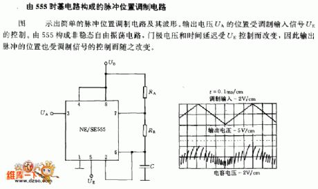
The pulse position modulating circuit composed of the 555 time-based circuit In the figure is the simple pulse position modulating circuit and its waveform. The position of the output voltage UA is controlled by the modulating input signal UE. The free oscillating circuit consists of 555, the gate voltage and the time delay is controlled by UE, so the position of the output pulse is changed by the control of the modulating signal.
(View)
View full Circuit Diagram | Comments | Reading(452)
| Pages:157/195 At 20141142143144145146147148149150151152153154155156157158159160Under 20 |
Circuit Categories
power supply circuit
Amplifier Circuit
Basic Circuit
LED and Light Circuit
Sensor Circuit
Signal Processing
Electrical Equipment Circuit
Control Circuit
Remote Control Circuit
A/D-D/A Converter Circuit
Audio Circuit
Measuring and Test Circuit
Communication Circuit
Computer-Related Circuit
555 Circuit
Automotive Circuit
Repairing Circuit