
Signal Processing
Index 144
SIREN_OSCILLATOR
Published:2009/6/18 23:25:00 Author:May

A CD4093 chip and a few components make up a siren oscillator, which drives power MOSFET T1. A 4-Ω speaker is driven directly from this device. The siren is enabled by a logic high applied to the ENABLE input. (View)
View full Circuit Diagram | Comments | Reading(3129)
SOUND_EFFECTS_GENERATOR
Published:2009/6/18 23:10:00 Author:May

The circuit consists of four parts: a binary counter, a D/A converter, a VCO, and an audio output amplifier. The speed at which the counter counts depends on the frequency of the output of the VCO, which in turn is determined by the output of the counter. That feedback loop gives this circuit its characteristic output.The initial frequency of oscillation is determined by potentiometer R11. The VCO first oscillates at a relatively low frequency, and it gradually picks up speed as the control voltage supplied by the D/A converter increases.The D/A converter is simply the group of resistors RI through R8. When none of IC1's outputs is ac-tive, little current will flow into the base of Q1, so the VCO's control voltage will be low. As more and more counter outputs become active, base current increases, and so does the VCO's frequency of oscillation.The VCO itself is composed of IC2-a, IC2-b, and Q1; the timing network is D1 through D4, C1, R10, and R11. The diode bridge functions basically as a voltage-controlled resistor. The buffer amplifier is made up of the four remaining gates from IC2, all wired in parallel. The volume is sufficient for experimental purnoses, but you might want to add an amplifier, speaker, or both. (View)
View full Circuit Diagram | Comments | Reading(2203)
ALARM_TONE_GENERATOR
Published:2009/6/18 23:00:00 Author:May
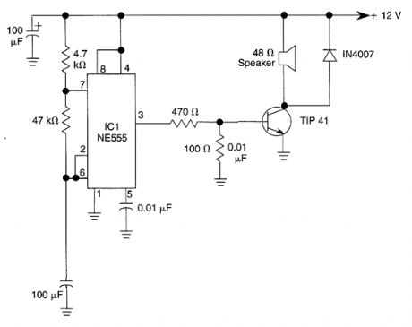
In this alarm tone generator, a TIP41 transistor is used as a speaker driver. R1, R2, and C1 determines the frequency which is 1400 Hz with the values shown. (View)
View full Circuit Diagram | Comments | Reading(2152)
PURE_SINE_WAVE_GENERATOR
Published:2009/6/18 21:55:00 Author:May

A TTL counter, an 8-channel analog multiplexer, and a fourth-order low-pass filter can generate 10- to 25-kHz sine waves with a THD better than -80 dB. The circuit cascades the two second-order, continuous-time Sallen-Key filters within IC3 to implement the fourth-order low-pass filter.To operate the circuit, choose the filter's cutoff frequency,fC, by tying IC3's D0 through D6 inputs to 5 V or ground. The cutoff frequency can be at 128 possible levels between 1 and 25 kHz, depending on those seven digital input levels. Because the circuit ties D0 through D6 to ground, fC equals 1 kHz. The 100-kΩ potentiometer adjusts the output level between VDD - 1.5 V and VSS + 1.5 V. (View)
View full Circuit Diagram | Comments | Reading(5)
SINE_WAVE_SHAPER
Published:2009/6/18 21:51:00 Author:May

Unlike most sine-wave shapers, this circuit is temperature stable. It varies the gain of a transcon-ductance amplifier to transform an input triangle wave into a good sine-wave approximation. (View)
View full Circuit Diagram | Comments | Reading(3)
SINE_WAVE_GENERATOR
Published:2009/6/18 21:50:00 Author:May

In this circuit, a square wave is filtered by a high-order low-pass filter so that a -3-dB frequency will eliminate most harmonics of the waveform. As a result, the filter outputs a fundamental sine wave. This method is applied to generate a sine wave by using a switched-capacitor filter (MAX292) (see the figure). This circuit offers wide frequency range (0.1 Hz to 25 kHz), low distortion, and con-stant output amplitude throughout the whole frequency range. (View)
View full Circuit Diagram | Comments | Reading(155)
SIMPLE_SINE_WAVE_GENERATOR
Published:2009/6/18 21:49:00 Author:May

A 555 timer operating in the astable mode generates the driving pulses and two 4518 dual BCD (binary coded decimal) counters provide the square waves. A TL081 op amp serves as an output buffer-amplifier, and potentiometers R1 and R2 are used in order to control the pulse's frequency and amplitude, respectively.The output-frequency range can be varied by changing CX. For example, a value of 0.1 μF gives a range from about 0.1 to 30 Hz, and avalue of 470 pF gives a range from about 10 Hz to 1.5 kHz. The maxirttum output frequency is 30 kHz. (View)
View full Circuit Diagram | Comments | Reading(2241)
1_Hz_SINE_WAVE_OSCILLATOR
Published:2009/6/18 21:46:00 Author:May

This circuit produces a 1-Hz sine wave using two op amps. A single-chip dual op amp could be used as well. (View)
View full Circuit Diagram | Comments | Reading(1250)
BATTERY_POWERED_SINE_WAVE_GENERATOR
Published:2009/6/18 21:45:00 Author:May

The quality of the sine wave depends on how closely you match the components in the twin-T network in the op amp's feedback loop. (View)
View full Circuit Diagram | Comments | Reading(1120)
WIEN_BRIDGE_SINE_WAVE_OSCILLATOR
Published:2009/6/18 21:43:00 Author:May

This Wien-bridge sine-wave oscillator uses a 2N3819 as an amplitude stabilizer. The 2N3819 acts as a variable-resistance element in the Wien bridge. (View)
View full Circuit Diagram | Comments | Reading(2)
SIMPLE_SINE_WAVE_OSCILLATOR
Published:2009/6/18 21:42:00 Author:May

Using an LC circuit,this CMOS oscillator generates slne waves. (View)
View full Circuit Diagram | Comments | Reading(2056)
HAM_BAND_VFO
Published:2009/6/18 3:54:00 Author:May

This basic VFO for the 3- to 6-MHz range is commonly used in amateur applications, using a Col-pitts circuit. For 5 to 5.5 MHz, C1 = C2 = 70 pF and for 3.5 to 4.0 MHz, use 1000 pF. C3 is typically 10 to 220 pF, depending on the frequency. C4, C5, and C6, together with C3, determine the frequency along with L1. C6 can be made up of several smaller values, paralleled to get the exact required value. (View)
View full Circuit Diagram | Comments | Reading(969)
REPEATER_TONE_BURST_GENERATOR
Published:2009/6/18 3:52:00 Author:May

Integrated circuit gates IC1-a and ICl-b form a monostable, whose time constant is determined by C2 and R3. When the transmitter is dekeyed (and then almost immediately rekeyed) point TX+ goes low and takes pin 1 low for a short time. This triggers the start of the timing period controlled by C2/R3, The capacitor C2, charges via R3 until the trigger point of gate ICl-b is reached. At this point, the monostable changes state and pin 3 goes low again. On the prototype, this time was about 700 ms. The pulse occurs each time after dekeying and it is normally inaudible. If, however, point TX+ goes high again (as in immediate rekeying) the monostable is still in the enabled state and the oscillations of ICl-c are present in the transmission. During this time period, the buffer gate, ICl-d, is enabled and the tone is therefore passed to the output. (View)
View full Circuit Diagram | Comments | Reading(926)
A_SHORTWAVE_PULSED_MARKER_OSCILLATOR
Published:2009/6/18 3:52:00 Author:May

A useful marker oscillator can be made using an NE555 to pulse the oscillator at an audio rate. This makes it easy to find the signal in the presence of interference. The crystal can be any suitable frequency from 1 to 30 MHz. (View)
View full Circuit Diagram | Comments | Reading(766)
NE6O2_RF_OSCILLATOR_CIRCUITS
Published:2009/6/18 3:50:00 Author:May

Just about any standard oscillator (such as a Colpitts or Hartley configuration) can be used to generate the LO (local oscillator) frequency needed by the NE602. (View)
View full Circuit Diagram | Comments | Reading(900)
TIME_DELAY_GENERATOR
Published:2009/6/18 3:00:00 Author:May

This circuit uses a charging capacitor and three comparators to read the voltage across it. (View)
View full Circuit Diagram | Comments | Reading(1472)
RF_SIGNAL_GENERATOR
Published:2009/6/18 2:42:00 Author:May

This circuit uses a VFO operating from 15 to 18 MHz (U1), which feeds a balanced mixer (U2). A fixed oscillator signal is mixed with this signal to generate an output from 0.4 to 33 MHz. FL1 and FL2 are low- and high-pass filters that are used to eliminate undesired mixer products. Amplifier U3/Q3 supplies up to 200 mV rms to the output jack. (View)
View full Circuit Diagram | Comments | Reading(2325)
65_MHz_VFO
Published:2009/6/18 2:40:00 Author:May

Fixed-value capacitors are disc ceramics. C1, C4, C5, C6, and C8 are NPO ceramic or polystyrene. C2 is a 25-pF ceramic trimmer and C3 is a 15-pF miniature air variable capacitor. The resistors are 1/4-W carbon film or composition. The RE chokes are miniature Mouser Electronics No. 43LR103 units. For L1, use 32 turns of #28 enamel wire on an Amidon Assoc. T50-6 (yeltow) toroid. L2 has 25 turns of #28 enamel wire on an Amidon Ft-37-61 ferrite toroid. (View)
View full Circuit Diagram | Comments | Reading(1193)
ONE_CHIP_AFSK_GENERATOR__
Published:2009/6/18 2:34:00 Author:May

Built around an XR2206 IC,this circuit wiⅡ generate AFSK signals in the 1000- to 3000-Hz range
(View)
View full Circuit Diagram | Comments | Reading(2754)
CURRENT_GENERATOR
Published:2009/6/18 1:59:00 Author:May

This circuit is useful for supplying constant current to test semiconductors. VOUT from U2 reads the voltage across the load connected to IOUT. R13 adjusts the supply compliance from 1 to about 18V. (View)
View full Circuit Diagram | Comments | Reading(653)
| Pages:144/195 At 20141142143144145146147148149150151152153154155156157158159160Under 20 |
Circuit Categories
power supply circuit
Amplifier Circuit
Basic Circuit
LED and Light Circuit
Sensor Circuit
Signal Processing
Electrical Equipment Circuit
Control Circuit
Remote Control Circuit
A/D-D/A Converter Circuit
Audio Circuit
Measuring and Test Circuit
Communication Circuit
Computer-Related Circuit
555 Circuit
Automotive Circuit
Repairing Circuit