
Signal Processing
Index 142
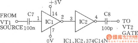
SSB signal generated by phase shift
Published:2011/7/28 3:26:00 Author:Ecco | Keyword: SSB signal , phase shift

Home SSB transmitter is a challenge to the HAM and a test to its own power. But up to now little HAM can self-make SSB transmitter, the main reason is the core components of the transmitter SSB-crystal filter and the matching crystal (such as crystal filters are equipped with 9MHz the 8998.5kHz, 9001.5kHz crystal) is difficult to purchase in the country, in this case, the phase shift method can generate SSB signals, comparing with the commonly used filter, but it has the advantages of easy make, low-cost, particularly the output frequency of VFO (should have a very high degree of frequency stability) can be directly taken as the firing frequency, it does not have to go through one or more frequency, greatly simplifying the whole circuit , the circuit is shown as the chart.
(View)
View full Circuit Diagram | Comments | Reading(1914)
LOW_FREQUENCY_ASTABLE
Published:2009/6/22 23:49:00 Author:May


By using a high-gain low-current transistor, such as the 2N3565, a pair of Darlington-connected transistors (2N3565 and 2N3904) can be used in a high-impedance configuration. (View)
View full Circuit Diagram | Comments | Reading(0)
Multi-frequency signal generator
Published:2011/7/28 3:22:00 Author:Ecco | Keyword: Multi-frequency , signal generator
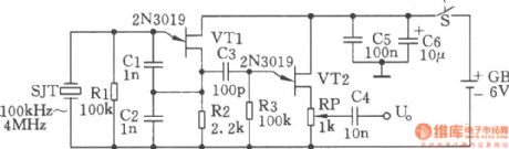
The chart shows the multi-frequency signal generator. SJT and VTl form a crystal oscillator. SJT is used as a quartz crystal equivalent inductance, the equivalent Q value is high, the other components and stray parameters have minimal effect on the oscillation frequency, so the frequency stability is high. VT2, etc. constitute a source follower to get low output impedance and an dampening effect to avoid the load to affect the crystal stability. In order to obtain more frequency signs to calibrate the receiver, it can use a square wave circuit shown as below. This circuit can instead of the the C3 in above figure, and be connected between the source of VT1 and grid of VT2, then it will generate rich harmonic signals (such as the l00kHz crystal can produce 30MHz harmonic signals). It can be used as frequency sign for calibrating general high frequency receiver.
(View)
View full Circuit Diagram | Comments | Reading(546)
LOW_DISTORTION_SINE_WAVE_OSCILLATOR
Published:2009/6/22 23:46:00 Author:May

C1,C2Min.Frequency Max.Frequency0.47μF 18 Hz 80 Hz 0.1μF 80 Hz 380 Hz 0.022μF 380 Hz 1.7 kHz0.0047μF 1.7 kHz 8 kHz0.002μF 4.4 kHz 20 kHz (View)
View full Circuit Diagram | Comments | Reading(0)
TONE_BURST_GENERATOR
Published:2009/6/22 23:45:00 Author:May

The burst length IS digitally controlled by inputs A,B,C,D.This input selects the necessary values ofR and C,The circuit shown in the figure generates a burst oftone followed by a silent period,then another tone burst is sounded and so forth,The timing of the tone bursts is digitally controlledvia the CD4066(IC2). A parts list for this circuit is given in the table.
IC1 556 dual timer(or two 555 timers)C5 0.047-μF capacitorIC2 CD4066 quad bilateral switchR1 100-kΩ, 1/4-W 5% resistorC1 1-μF,25-V electrolytic capacitorR2,R4 220-kΩ, 1/4-W 5% resistorC2 4.7-μF, 25-V electrolytic capacitor R3 680-kΩ, 1/4-W 5% resistorC3 10-μF, 25-V electrolytic capacitor R5 12-kΩ, 1/4-W 5% resistorC4,C60.01-μF capacitor R6 4.7-kΩ, 1/4-W 5% resistor (View)
View full Circuit Diagram | Comments | Reading(0)
BASIC_LM3909_AUDIO_OSCILLATOR
Published:2009/6/22 23:42:00 Author:May

The LM3909's oscillator frequency can be fine-tuned by adding a resistor to a basic circuit. (View)
View full Circuit Diagram | Comments | Reading(757)
ONE_TRANSISTOR_PHASE_SHIFT_OSCILLATOR
Published:2009/6/22 23:41:00 Author:May

A single transistor is used as an active element in an RC phase shift oscillator. (View)
View full Circuit Diagram | Comments | Reading(2511)
QUAD_TONE_OSCILLATOR
Published:2009/6/22 23:40:00 Author:May

A quad op amp (TL084, etc.) can be used to produce four audio tone generators for use in a test setup. The circuit uses a 12-V supply. (View)
View full Circuit Diagram | Comments | Reading(0)
EASILY_TUNED_SINE_WAVE_OSCILLATOR
Published:2009/6/22 23:39:00 Author:May

The circuit will provide both a sine-and square-wave output for frequencies from below 20 Hz to above 20 kHz. The frequency of oscillation is easily tuned by varying a single resistor. This is a considerable advantage over Wien bridge circuits, where two elements must be tuned simultaneously to change frequency. Also, the output amplitude is relatively stable when the frequency is changed.An operational amplifier is used as a tuned circuit, driven by square wave from a voltage comparator. Frequency is controlled by R1, R2, C1, C2, and R3, with R3 used for tuning. Tuning the filter does not affect its gain or bandwidth, so the output amplitude does not change with frequency. A comparator is fed with the sine-wave output to obtain a square wave. The square wave is then fed back to the input of the tuned circuit to cause oscillation. Zener diode, D1, stabilizes the amplitude of the square wave fed back to the filter input. Starting is ensured by R6 and C5, which provide dc negative feedback around the comparator. This keeps the comparator in the active region (View)
View full Circuit Diagram | Comments | Reading(0)
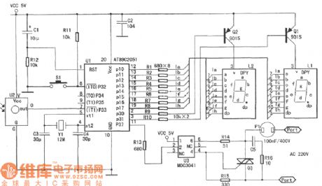
The manufacturing circuit of infrared reception controller
Published:2011/7/21 3:34:00 Author:Seven | Keyword: manufacturing circuit, infrared reception controller
View full Circuit Diagram | Comments | Reading(455)
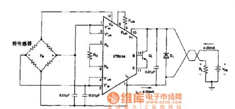
The bridge sensor over-voltage wave protection circuit
Published:2011/7/21 2:28:00 Author:Seven | Keyword: bridge sensor, protection circuit
View full Circuit Diagram | Comments | Reading(417)
SINGLE_CHIP_MESSAGE_SYSTEM
Published:2009/6/22 23:35:00 Author:Jessie

The ISD1016 is a complete analog audio record/playback system on a chip. The analog signal is sampled and the samples stored in an EEPROM as analog levels. Upon playback, the analog data is read out and amplified. Up to 16 seconds of data(audio)can be stored. (View)
View full Circuit Diagram | Comments | Reading(1429)
VIDEO,POWER,AND_CHANNEL_SELECT_SIGNAL_CARRIER
Published:2009/6/22 23:01:00 Author:Jessie

In the video system of Figs. A and B, a single coaxial cable carries power to the remote location, selects one of eight video channels, and returns the selected signal. The system can choose one of several remote surveillance-camera signals, for example, and display the picture on a monitor near the interface box.
The heart of the multiplexer box (A) is a combination 8-channel rnultiplexer and amplifier (ICl). C11 couples the multiplexer's baseband video output to the coax, and L1 decouples the video from dc power arriving on the same line. This power-approximately 30 mA at 10 V-supplies all circuitry in the multiplexer box.
In interface box (B), a desired channel is encoded by three bits, set either by switches as shown or by an applied digital input. Momentary depression of the send button triggers clownconverter IC1 and gated oscillator IC2A to initiate a channel-selection burst. (View)
View full Circuit Diagram | Comments | Reading(2036)
PROGRAMMABLE_RESISTOR_CIRCUIT
Published:2009/6/22 22:49:00 Author:Jessie

IC1 CD4066 quad bilateral switchC1 0.1-μF capacitorRI 10-kΩ, 1/4-W 5% resistorR2 4.7-kΩ, 1/4-W 5% resistorR3 2.2-kΩ, 1/4-W 5% resistorR4 1-kΩ, 1/4-W 5% resistorR5 1-MΩ, 1/4-W 5% resistor
A programmable resistor can replace a potentiometer or fixed resistor. Remember that the ON resistance of IC1 might have to be taken into account in some applications. (View)
View full Circuit Diagram | Comments | Reading(2194)
TRAFFIC_LIGHT_SEQUENCER_CIRCUIT
Published:2009/6/22 22:36:00 Author:May
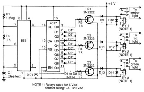
This circuit uses a 555 timer to drive a 4017 counter. The counter outputs drive transistor relay drivers. Time lights on can be proportioned by changing connections of outputs of counter. (View)
View full Circuit Diagram | Comments | Reading(4859)
ACOUSTIC_FIELD_GENERATOR
Published:2009/6/22 22:35:00 Author:May
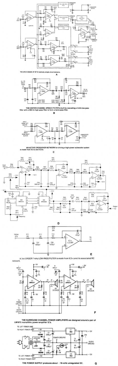
Referring to the simplified schematic in A, the AFG is made up of 10 relatively simple circuit el-ements. ICl-c and ICl-d are configured as unity-gain noninverting buffer amplifiers.
The summing (L+R) amplifier, IC2-c, combines equal amounts of the left and right signals, via R14 and R15, to develop a total composite signal. Left- and right-channel signals are applied equally through R13 and R12 to IC2-d, the difference (L-R) decoder. Any common to both channels is canceled by IC2-d, which exactly balances the inverting and noninverting gains of the amplifier for a perfect null.
The stereo width-enhancement circuit made up from IC1-a and IC-b works similarly to the (L-R) decoder, except that C25 and C26 have been added in the inverting inputs of each op amp. IC1-b de-velops the left wide signal because its inverting and noninverting inputs are connected to the left
and right channels opposite that of IC1-a. The output of the width-enhancement circuit is routed to 54, which selects either the wide or the bypass signal for feeding the front-channel amplifier.
The center-channel dialogue filter is built by cascading a 3-kHz low-pass filter with a 3-Hz high-pass filter to form a band-j:ass filter. It has a sharp -18 dB/octave cutoff, a flat voltage and power fre-quency response, and minimum phase change within the passband.
In C, IC3-a and IC3-b form an active crossover network for driving a subwoofer. IC3-a sums sig-nals from the left- and right-channel buffer amps, it inverts the summed signal 180 degrees, and pro-vides a low driving impedance for the following filter stage. IC3-b and its associated RC network form a 75-Hz, 3rd-order low-pass filter. The filter inverts the signal another 180 degrees, so the signal that appears across R79 (which is the output-level control) is back in phase with the original input signal.
The delay section of the AFG, shown in D, is built around the MN3008 bucket brigade device (BBD), and the MN3101 two-phase variable-frequency clock generator. The amount of delay re-quired in this system varies between approximately 5 to 35 milliseconds. The delay time of a BBD is equal to the number of stages divided by twice the clock frequency. Values were chosen for R53, R54, R77, and C44, to produce a clock frequency, adjustable via R77, which varies from about 30 kHz to 130 kHz.
In A, S1 selects the signal to be delayed, either the difference signal (L-R) from IC2-djn the ma-Lrix mode or the sum signa! (L-R) from IC2-c in the concert mode. The selected signal is fed from S1 to the delay section (D) where IC4-d is configured as an inverting amplifier; R75 adjusts the gain between unity and X3: Integrated circuits IC4-a and IC4-b, along with their assoicated RC networks: are identical 3rd-order 15-kHz low-pass filters. Cascading two filters produces a very sharp cut off (-36 dB per octave). Potentiometer R76 adjusts the bias voltage required by the BBD to exactly one half the supply voltage, as required.
The power suppty of the AFG, shown in G, is of conventional design. A 25-V center-tapped trans-former, along with diodes D1 and D2, produces about t18-V unregulated dc. 1bro 2200-μF filter capacitors provide ample energy storage to meet the high-current demands of the audio output amplifier ICs during high output peaks. (View)
View full Circuit Diagram | Comments | Reading(1281)
Low cost Wien oscillator composed of F007
Published:2011/7/28 3:16:00 Author:Ecco | Keyword: Low cost , Wien oscillator

The chart shows the low cost Wien oscillator circuit. One hand, the circuit can avoid the problem of having to adopt expensive inductors in the general oscillator circuits. On the other hand,it can also avoid using double-potentionmeter to adjust frequency in the Wien bridge oscillators. It only uses a potentiometer to adjust the frequency, so the cost is lower. The adjusting frequency range is small, although there are some defects, it can still be used when it needs small frequency range, and the circuit is stable. (View)
View full Circuit Diagram | Comments | Reading(594)
Wien bridge sine-wave generator
Published:2011/7/28 2:19:00 Author:Ecco | Keyword: Wien bridge , sine-wave, generator

Oscillation frequency of the circuit shown in the figure is about lkHz, and it uses the regulator 2DW78 to stabilize amplitude. Ifl. 5kΩ resistors in the bridge isreplaced bycoaxial double potentiometer, the band switch needs to access different capacitors, the output signal frequency can be adjusted continuously. The maximum frequency of oscillation circuit is decided by the characteristics of operational amplifier F007. And the greater resistance, capacitance on low frequency end will cause instability or leakage, so the input impedance of operational amplifier should be as high as possible.
(View)
View full Circuit Diagram | Comments | Reading(796)
SOUND_SUBCARRIER_GENERATOR
Published:2009/6/22 17:59:00 Author:May


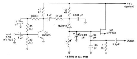
This circuit will generate an FM sound subcarrier at 4.5 or 10.7 MHz for FM and TV IF testing and alignment. Q1 is an audio amplifier and Q2 is a VCO rrtodulated by an MV2112 varactor. Devia-tion up to 1% of frequency can be obtained. L is chosen to resonate with the circuit capacitance to either 4.5 or 10.7 MHz. The values will be around 2 to 10 pH, depending on the frequency. (View)
View full Circuit Diagram | Comments | Reading(777)
2.5kHz Wien bridge signal generator
Published:2011/7/28 2:16:00 Author:Ecco | Keyword: 2.5kHz , Wien bridge , signal generator
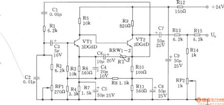
The 2.5kHz signal generator is a RC Wien low-bridge oscillator circuit, it is shown as the chart. Transistor VTl, VT2 form second order direct coupled amplifier.By inputting the bootstrap can improve the circuit's input impedance and decrease the impact on RC shift circuit. Connecting a T-attenuation device on output end can meet the requirement of inpedance output on one hand, on the other hand it also can reduce the influence of load on Rc shift circuit. Taking the measures, the oscillator frequency stability is mainly decided by the RC phase shift components. Rc components with low temperature coefficient is used, thus, the oscillator frequency is relatively stable (25 ℃ ± 15 ℃, the frequency changing ≤ ± 5Hz).
(View)
View full Circuit Diagram | Comments | Reading(1387)
| Pages:142/195 At 20141142143144145146147148149150151152153154155156157158159160Under 20 |
Circuit Categories
power supply circuit
Amplifier Circuit
Basic Circuit
LED and Light Circuit
Sensor Circuit
Signal Processing
Electrical Equipment Circuit
Control Circuit
Remote Control Circuit
A/D-D/A Converter Circuit
Audio Circuit
Measuring and Test Circuit
Communication Circuit
Computer-Related Circuit
555 Circuit
Automotive Circuit
Repairing Circuit