Signal Processing
The circuit design reference diagram
Published:2011/7/1 23:54:00 Author:Borg | Keyword: circuit design, reference diagram | From:SeekIC

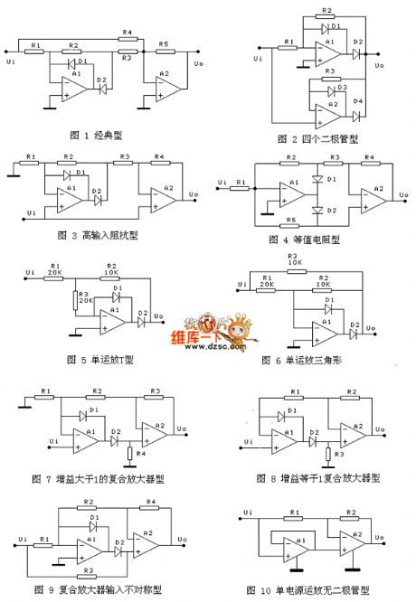
The precise full-wave rectifier circuit in the figure is named by myself, which is only for distinguishing; unless there are special instructions, or the gains are all designed according to 1. In figure 1 is the most classical circuit, whose virtue is that it can connect with a filter capacitor in the parallel way on R5. The coupling relation is R1=R2, R4=R5=2R3. It can also adjust the gain by changing R5. The circuit in figure 2 characterizes few resistors, which only requires R1=R2. The circuit in figure 3 characterizes high input impedance, the coupled resistor requires R1=R2, R4=2R3. All the coupled resistors in figure 4 are the same, and the gain can be adjusted by changing R1.
Reprinted Url Of This Article:
http://www.seekic.com/circuit_diagram/Signal_Processing/The_circuit_design_reference_diagram.html
Print this Page | Comments | Reading(3)

Article Categories
power supply circuit
Amplifier Circuit
Basic Circuit
LED and Light Circuit
Sensor Circuit
Signal Processing
Electrical Equipment Circuit
Control Circuit
Remote Control Circuit
A/D-D/A Converter Circuit
Audio Circuit
Measuring and Test Circuit
Communication Circuit
Computer-Related Circuit
555 Circuit
Automotive Circuit
Repairing Circuit
Code: