
Signal Processing
Index 135
SIMPLE_ULTRASONIC_GENERATOR
Published:2009/6/24 21:35:00 Author:May
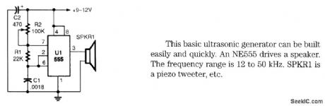
This basic ultrasonic generator can be built easily and quickly. An NE555 drives a speaker.The frequency range is 12 to 50 kHz. SPKRI is a piezo tweeter, etc. (View)
View full Circuit Diagram | Comments | Reading(2141)
CMOS_VFO
Published:2009/6/24 21:31:00 Author:May

The circuit shown has a frequency range of 2 Hz to 30 kHz. R2 is a linear or log potentiometer. (View)
View full Circuit Diagram | Comments | Reading(0)
CRYSTAL_OSCILLATOR
Published:2009/6/24 21:28:00 Author:May

Circuit NotesStable VXO using 6-or 8-MHz crystals uses a capacitor and an inductor to achieve frequency pulling on either side of series resonance. (View)
View full Circuit Diagram | Comments | Reading(0)
SIMPLE_TTL_CRYSTAL_OSCILLATOR
Published:2009/6/24 21:25:00 Author:May

Circuit NotesThis simple and cheap crystal oscillator comprises one third of a 7404, four resistors and a crystal. The inverters are biased into their linear regions by RI to R4, and the crystal provides the feedback. Oscillation can only occur at the crystals fundamental frequency. (View)
View full Circuit Diagram | Comments | Reading(10039)
PRECISION_AUDIO_FREQUENCY_GENERATOR
Published:2009/6/24 21:25:00 Author:May

The precision audio-frequency generator consists of several subcircuits-an audio-amplifier/filter circuit, an automatic level control, a variable voltage-controlled oscillator, a frequency divider circuit, an integrator, and an audio output amplifier.
An electret microphone element is used to pick up the audio tone produced by the instrument. That signal is then fed to an amplifier/filter/level-controlled circuit and output via channel 1 (CH1) to an oscilloscope for display.
The variable voltage-controlled oscillator (VCO) is used to produce a signal offrom less than 10 kHz to more than 99 kHz. The VCO output is fed to a digital frequency counter for display, and is also routed to a chain of frequency dividers, where the signal is divided by 10, 100, or 1,000, depending on the setting of a selector switch.
From there, the selected signal frequency divides along two paths; one going to CH2 (which feeds the oscilloscope's sweep synchronization input) and to an integrator that converts the square-wave output of the divider into a triangular waveform. The output of the integrator is then amplified and fed to a set of stereo headphones via an audio output jack.
One section of the precision audio-frequency generator uses an electret microphone element to pick up audio from the piano. That signal is then processed and sent to one channel of a dual-trace oscilloscope. The other section of the circuit is used to produce a variable-frequency signal that is fed to a digital frequency counter and, after conditioning, is presented to the second channel of the scope and output to a set of stereo headphones. (View)
View full Circuit Diagram | Comments | Reading(2069)
VARIABLE_WIEN_BRIDGE_OSCILLATOR
Published:2009/6/24 21:15:00 Author:May

This circuit uses a single potentiometer to tune a 300- to 3000-Hz range. A FET op amp is used at A1 and A2. The upper frequency limit is determined by the gain-bandwidth product of the op amps. (View)
View full Circuit Diagram | Comments | Reading(0)
BASIC_OSCILLATOR_CIRCUITS
Published:2009/6/24 21:12:00 Author:May


Five basic types of LC oscillators are shown. The frequency can be changed by using the formula:where Leffective =equivalent inductance Ceffective =equivalent capacitance (View)
View full Circuit Diagram | Comments | Reading(0)
PRECISION_LF_OSCILLATOR
Published:2009/6/24 21:07:00 Author:May

Using R1, R7, and D1 to preset C1 to one third of the supply voltage, this circuit avoids a longer first cycle period than subsequent cycles. (View)
View full Circuit Diagram | Comments | Reading(0)
GATED_1_kHz_OSCILLATOR(NORMALLY_ON)
Published:2009/6/24 21:06:00 Author:May

This gated 1-kHz oscillator offers press-to-turn-off' operation, A, and waveforms at the out-put of pin 3 and across C1, B. (View)
View full Circuit Diagram | Comments | Reading(0)
GATED_1_kHz_OSCILLATOR(NORMALLY_OFF)
Published:2009/6/24 21:05:00 Author:May

This gated 1-kHz oscillator offers press-to-turn-on operation, A, and waveforms at the out-put of pin3 and across C1, B. (View)
View full Circuit Diagram | Comments | Reading(0)
TTL_OSCILLATOR_FOR_1_MHz_10_MHz
Published:2009/6/24 21:01:00 Author:May
View full Circuit Diagram | Comments | Reading(0)
96_MHz_CRYSTAL_OSCILLATOR
Published:2009/6/24 21:00:00 Author:May


Circuit NotesBy usmg a crystal between 27.5 and 33 MHz,the 3rd harmonic will deliver between82.5 and 99 MHz. (View)
View full Circuit Diagram | Comments | Reading(0)
OVERTONE_CRYSTAL_OSCILLATOR
Published:2009/6/24 20:49:00 Author:May

The crystal element in this circuit is con-nected directly between the base and ground.Capacitor C1 is used to improve the feedback due to the internal capacitances of the transis-tor. This capacitor should be mounted as close as possible to the case of the transistor. The LC tank circuit in the collector of the transistor is tuned to the overtone frequency of the crystal.The emitter resistor capacitor must have a capacitive reactance of approximately 90 ohms at the frequency of operation. The tap on induc-tor L1 is used to match the impedance of the collector of the transistor. In most cases, the optimum placement of this tap is approximately one-third from the cold end of the coil. The placement of this tap is a trade-off between stability and maximum power output. The out-put signal is taken from a link coupling coil, L2, and operates by transformer action. (View)
View full Circuit Diagram | Comments | Reading(0)
HIGH_FREQUENCY_CRYSTAL_OSCILLATOR
Published:2009/6/24 20:42:00 Author:May
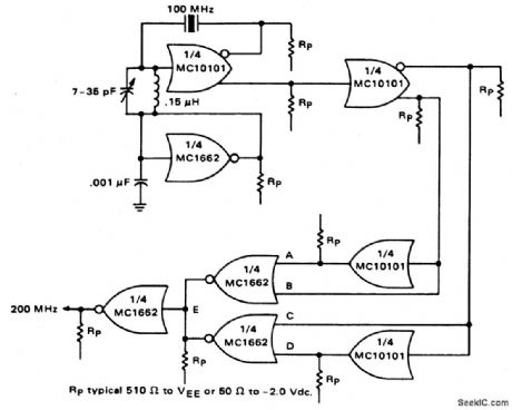
Circuit NotesOne section of the MC10101 is connected as a 100 MHz crystal oscillator with the crystal in series with the feedback loop. The LO tank circuit tunes the 100 MHz harmonic of the crystal and may be used to calibrate the circuit to the exact frequency. A second section of the MC10101 buffers the crystal oscillator and gives complementary 100 MHz signals. Thefrequency doubler consists of two MC10101 gates as phase shifters and two MC1662 NOR gates. For a 50% duty cycle at the output, the delay to the true and complement 100 MHz signals should be 90'. This may be built pre-cisely with 2.5 ns delay lines for the 200 MHz output or approximated by the two MC10101 gates as shown. (View)
View full Circuit Diagram | Comments | Reading(0)
LOW_FREQUENCY_RELAY_OSCILLATOR
Published:2009/6/24 5:42:00 Author:May

Depending on the value of C and the resistance of the relay coil, and the difference in pull-in and drop-out voltage, this circuit will oscillate at a low frequency. R limits in rush current to capacitor C to a level that the relay contacts can handle. Typically, for a 400-Ω relay, R can be 20 to 440 ohms.Flash rate is approximately 1 cycle/second, depending on the relay. (View)
View full Circuit Diagram | Comments | Reading(0)
SIGNAL_TRACER
Published:2009/6/24 21:13:00 Author:Jessie

This circuit uses a simple detector-audio am-plifier. The output can be connected to head-phones or another audio amplifier. (View)
View full Circuit Diagram | Comments | Reading(2703)
REDUCING_RIPPLE_IN_A_SWITCHING_VOLTAGE_REGULATOR
Published:2009/6/24 5:17:00 Author:May

Simple additional circuitry that consists of relatively small components can reduce the output ripple by a factor of about 10. The additional components are indicated by the dashed lines.A current opposing the ripple is injected into the filter capacitor. The essence of the present technique is to inject, into this capacitor, a cur-rent opposite to that which already flows into this capacitor. A small additional winding, L1, in inductor L0 provides transformer coupling to generate the current that opposes the original ripple current. The circuit from L1 through C0 is completed by a small additional extemal inductor L2 and coupling capacitor C1. (View)
View full Circuit Diagram | Comments | Reading(493)
NOISE_GENERATOR
Published:2009/6/24 5:12:00 Author:May

This noise generator uses a Zener diode. The transistors are part of the LM389. (View)
View full Circuit Diagram | Comments | Reading(0)
RELAY_INTERFACE_TO_RC_RECEIVERS
Published:2009/6/24 4:30:00 Author:Jessie
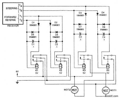
You can add relays to some inexpensive RC receivers to operate your own chassis. (View)
View full Circuit Diagram | Comments | Reading(586)
TWO_CHIP_AM_RECEIVER
Published:2009/6/24 4:29:00 Author:Jessie
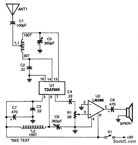
This receiver is comprised of a TDA7000 single-chip FM receiver (U1), an LM386 low-voltage audio-power amplifier (U2), a pair of hand-wound coils (L1 and L2), and a few additional components.L1 and L2 are 100 tums of #28 wire on toroidal cores (about 240 μH each). L1 is tapped at 30 turns. (View)
View full Circuit Diagram | Comments | Reading(2512)
| Pages:135/195 At 20121122123124125126127128129130131132133134135136137138139140Under 20 |
Circuit Categories
power supply circuit
Amplifier Circuit
Basic Circuit
LED and Light Circuit
Sensor Circuit
Signal Processing
Electrical Equipment Circuit
Control Circuit
Remote Control Circuit
A/D-D/A Converter Circuit
Audio Circuit
Measuring and Test Circuit
Communication Circuit
Computer-Related Circuit
555 Circuit
Automotive Circuit
Repairing Circuit