
Signal Processing
Index 124
ASTABLE_OSCILLATOR
Published:2009/7/1 19:56:00 Author:May

Circuit for astable operation of 555 timer provides completely independent ON and OFF times. Time constant for one mode is 1.1 RCC2 and for other mode is 1.1 RCC3. Free-running period is sum of these time constants.-J. P. Carter, Astable Operation of IC Timers Can Be lmproved, EDN Magazine, June 20, 1973, p 83. (View)
View full Circuit Diagram | Comments | Reading(0)
LOG_SWEEP
Published:2009/7/24 3:45:00 Author:Jessie
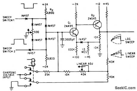
Resistance coupling in feed-back loop permits positive-going as well as negative-going waveforms. Circuit gives choice of logarithmic, exponential, or linear sweep output. Relay switches between linear and long sweep.-J. Curry and W. Sander, Bootstrap Generates Logarithmic Sweeps, Electronics, 33:52, p 60. (View)
View full Circuit Diagram | Comments | Reading(690)
Strobed_strain_gauge_conditioner
Published:2009/7/24 3:44:00 Author:Jessie

Fig. 14-14 This circuit also provides an output from a strain-gauge transducer on a sampled basis (to minimize power consumption), as does the circuit of Fig. 14-13. However, the Fig. 14-14 circuit is designed to remain in the quiescent state for long periods with relatively brief on-times, actuated by a sample or strobe command. A typical application would be for remote weight information in storage tanks, where weekly readings are sufficient. Quiescent current is about 150μA and on-state current about 50 mA. The output-trim pot scales the circuit for 3-mV/V-type strain-gauge transducers. Linear Technology Linear Applications Handbook 1990, p AN23-4. (View)
View full Circuit Diagram | Comments | Reading(1143)
Magnetic_pickup_signal_conditioner
Published:2009/7/24 4:00:00 Author:Jessie

Fig. 14-16 This circuit uses an LM2907 as a very simple signal conditioner for a magnetic pickup. This basic configuration provides a low-impedance output voltage that is proportional to input frequency. The linearity of this voltage is typically better than 0.3% of full scale. No calibration is required. National Semiconductor Linear Applications Handbook, 1991.p. 423. (View)
View full Circuit Diagram | Comments | Reading(2084)
Acoustic_thermometer
Published:2009/7/24 3:59:00 Author:Jessie


Fig. 14-15 Acoustic thermometry is used where extremes in operating temperature are encountered, such as in cryogenics and nuclear reactors. The transducer is composed of Polaroid ultrasonic material, mounted at one end of a sealed, 6-in long Invar tube. The medium inside the tube is dry air. The transducer can be considered a capacitor, composed of an insulating disc with conductive coating on each side. Each clock pulse causes mechanical movement of the disc, and ultrasonic energy is emitted. The clock pulse simultaneously resets the 74C74 output flip-flop. The ultrasonic energy travels down the tube, bounces off the far end, and returns to the transducer, causing mechanical displacement of the transducer. This shifts the transducer capacitance, resetting the 74C74 through A2 and C1. The 74C74 output pulse represents the transit time down the tube and it varies with the temperature, according to the equation:
C=331, √5T/273 meters/second, where C=speed of sound.
The pulse width (time between set and reset) can be converted into desired temperature information with a monitoring processor. Linear Technology. Linear Applications Handbook 1990. p AN7-5, (View)
View full Circuit Diagram | Comments | Reading(0)
CRYSTAL_STABILIZED_IC_TIMER_CANPROVIDE_SUBHARMONIC_FREQUENCIES
Published:2009/7/1 3:59:00 Author:May

View full Circuit Diagram | Comments | Reading(525)
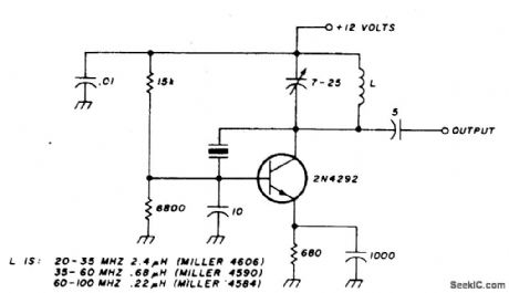
HIGH_FREQUENCY_SIGNAL_GENERATOR
Published:2009/7/1 3:54:00 Author:May

A tapped-coil Colpitts oscillator is used at Q1 to provide four tuning ranges from 1.7 to 3.1 MHz, 3.0 to 5.6 MHz, 5.0 to 12 MHz and 11.5 to 31 MHz. A Zener diode (D2) is used at Q1 to lower the operating voltage of the oscillator. A small value capaci-tor is used at C5 to ensure light coupling to the tuned circuit. Q2 is a source-follower buffer stage. It helps to isolate the oscillator from the generator-output load. The source of Q2 is broadly tuned by means of RFC1. Energy from Q2 is routed to a fed-back, broadband class-A amplifier. A 2 dB attenuator is used at the output of T1 to provide a 50 ohm termination for Q3 and to set the generator-output impedance at 50 ohms.C16, C17 and RFC2 form a brute-force RF decoupling network to keep the generator energy from radiating outside the box on the 12 V supply. (View)
View full Circuit Diagram | Comments | Reading(1283)
CRYSTAL_CONTROLLED_OSCLLATOR_OPERATES_FROM_ONE_MERCURY_CELL
Published:2009/7/1 3:51:00 Author:May

The circuit is powered by a single 1.35 V mercury cell and provides a 1 V squarewave output. As shown, the crystal is a tuned circuit between transistors Q1 and Q2, which are connected in the common-emitter configuration. Positive feedback provided by means of R permits oscillation. The signal at the collector of Q2 is squared by Q3, which switches between cutoff and saturation. R7 permits short-circuit-proof operation. (View)
View full Circuit Diagram | Comments | Reading(840)
HIGH_FREQUENCY_CRYSTAL_OSCILLATOR
Published:2009/7/1 3:48:00 Author:May

A high speed oscillator is possible by combining an MECL 10 K crystal oscillator with an MECL III frequency doubler as shown. One section of the MC10101 is connected as a 100 MHz crystal oscillator with the crystal in series with the feedback loop. The LC tank circuit tunes the 100 MHz harmonic of the crystal and may be used to calibrate the circuit to the exact frequency. A second section of the MC10101 buffers the crystal oscillator and gives complementary 100 MHz signals. The frequency doubler consists of two MC10101 gates as phase shifters and two MC1662 NOR gates. For a 50% duty cycle at the output, the delay to the true and complement 100 MHz signals should be 90°. This may be built precisely with 2.5 ns delay lines for the 200 MHz output or approximated by the two MC10101 gates. The gates are easier to incorporate and cause only a slight skew in output signal duty cycle. The MC1662 gates combine the 4 phase 100 MHz signals as shown in Figure B. The outputs of the MC1662's are wire-OR connected to give the 200 MHz signal. MECL III gates are used because of the bandwidth required for 200 MHz signals. One of the remaining MC1662 gates is used as a Vgg bias generator for the oscillator. By connecting the NOR output to the input, the circuit stays in the center of the logic swing or at VBB. A 0.001 μF capacitor ensures the VBB circuit does not oscillate. (View)
View full Circuit Diagram | Comments | Reading(0)
CRYSTAL_CONTROLLED_OSCILLATOR
Published:2009/7/1 3:43:00 Author:May

View full Circuit Diagram | Comments | Reading(0)
COLPITTS_OSCILLATOR
Published:2009/7/1 3:42:00 Author:May

Bias for the pnp bipolar transistor is provided by resistor voltage divider network R1/R2. The collector of the oscillator transistor is kept at ac ground by capacitor C5, placed close to the transistor. Feedback is provided by capacitor voltage divider C2/C3. (View)
View full Circuit Diagram | Comments | Reading(0)
Instrumentation_amplifier_with_300_V_common_mode_range
Published:2009/7/24 4:06:00 Author:Jessie

Fig. 14-20 This circuit will withstand common-mode voltages of 1300 V and provide a CMRR of 160 dB or greater (see chapter 10 for coverage of common-mode voltages and CMRR). To trim, adjust R1 for 93 Hz at the LM301A output. Then, adjust the gain-trim pot for the desired gain. This amplifier is particularly useful for transducer signal conditioning, where high common-mode voltages mightexist. Linear Technology Linear Applications Handbook, 1990. p. AN6-2. (View)
View full Circuit Diagram | Comments | Reading(577)
OVERTONE_CRYSTAL_OSCILLATOR
Published:2009/7/1 3:40:00 Author:May
This oscillator is designed for overtone crystals in the 20-100 MHz range operating in the third and fifth mode. Operating frequency is determined by the tuned circuit. (View)
View full Circuit Diagram | Comments | Reading(0)
Capacitive_transducer_signal_conditioner
Published:2009/7/24 4:05:00 Author:Jessie

Fig. 14-19 This circuit uses an LM2907 to condition the output of a capacitive transducer, and to mix this output with another variable. If the other signal is fixed at 60-Hz, as shown, then the output is proportional to the capacitive-transducer output only. If the other signal is variable, the transducer acts as a multiplier. For example, in flow-measurement indicators, the input frequency can be a variable that depends on flow rate, such as a signal generated from a paddle wheel, propeller, etc. The capacitive-transducer can be an indication of orifice size or aperture size (such as a throttle). The product of these two indicates volume flow, where the output voltage is proportional to size times rate. A thermistor can be added to R1 to convert the volume flow to mass flow. A combination of these signal-conditioned inputs, including control voltage on the supply, can be used to provide complex analog functions, where several variable or fixed factors must be multiplied. National Semiconductor Linear Applications Handbook, 1991. p. 432. (View)
View full Circuit Diagram | Comments | Reading(1734)
Gasoline_engine_signal_conditioner
Published:2009/7/24 4:04:00 Author:Jessie

Fig. 14-18 This circuit uses an LM2907 to condition the signals between a gasoline engine and a tachometer. The simple circuit can be set for any number of cylinders by linking the appropriate timing resistor, as shown. The 500-Ω calibration pot is set so that 6000 rpm produces a full-scale indication on a 10-mA meter movement.the zener and resistor ale added as a safety precaution against transients. National Semicondutor Applications Handbook, 1991. p 429 . (View)
View full Circuit Diagram | Comments | Reading(1565)
LOW_FREaUENCY_CRYSTAL_OSCILLATOR_10kHz_to_150_kHz
Published:2009/7/1 3:38:00 Author:May


C1 in series with the crystal may be used to adjust the oscillator output frequency. Value may range between 20 pF and 0.01 μF, or may be a trimmer capacitor and will approximately equal the crystal load capacitance. X values are approximate and can vary for most circuits and frequencies; this is also true for resistance values. Adequate power supply decoupling is required; local decoupling capacitors near the oscillator are recommended. All leads should be extremely short in high frequency circuits. (View)
View full Circuit Diagram | Comments | Reading(753)
CRYSTAL_OSCILLATOR_PROVIDES_LOW_NOISE
Published:2009/7/1 3:35:00 Author:May

The oscillator delivers an output of high spectral purity without any substantial sacrifice of the usual stability of a crystal oscillator. The crystal in addition to determining the oscillator's frequency, is used also as a low-pass filter for the unwanted harmonics and as a bandpass filter for the sideband noise. The noise bandwidth is limited to less than 100 Hz. All higher harmonics are substantially suppressed-60 dB down for the third harmonic of the 4-MHz fundamental oscillator frequency. (View)
View full Circuit Diagram | Comments | Reading(728)
IC_COMPATIBLE_CRYSTAL_OSCILLATOR
Published:2009/7/1 3:33:00 Author:May

Resistors R1 and R2 temperature-stabilize the NAND gates; they also ensure that the gates are in a linear region for starting. Capacitor C1 is a dc block; it must have less than1/10 ohm impedance at the operating frequency. The crystal runs in a series-resonant mode. Its series resistance must be low; AT-cut crystals for the 1-to 10-MHz range work well. The output waveshape has nearly a 50% duty cycle, with chip-limited rise times. The circuit starts well from 0°to 70℃. (View)
View full Circuit Diagram | Comments | Reading(791)
PRECISE_WAVE_GENERATOR
Published:2009/7/1 3:29:00 Author:May

The positive and negative peak amplitude is controllable to an accuracy of about ±0.01 V by a dc input. Also, the output frequency and symmetry are easily adjustable. The oscillator consists of an integrator and two comparators-one comparator sets the positive peak and the other the negative peak of the triangle wave. If R1 is replaced by a potentiometer, the frequency can be varied over at least a 10 to 1 range without affecting amplitude. Symmetry is also adjustable by connecting a 50 kΩ resistor from the inverting input of the LM118 to the arm of the 1 kΩ potentiometer. The ends of the potentiometer are connected across the supplies. Current for the resistor either adds or subtracts from the current through R1,changing the ramp time. (View)
View full Circuit Diagram | Comments | Reading(560)
SINGLE_SUPPLY_FUNCTION_GENERATOR
Published:2009/7/1 3:23:00 Author:May


The circuit has both square-wave and triangle-wave output. The left section is similar in function to a comparator circuit that uses positive feedback for hysteresis. The inverting input is biased at one-half the VCC voltage by resistors R4 and R5. The output is fed back to the non-inverting input of the first stage to control the frequency. The amplitude of the square wave is the output swing of the first stage, which is 8 V peak-to-peak.The second stage is basically an op amp integrator. The resistor R3 is the input element and capacitor C1 is the feedback element. The ratio RI/R2 sets the amplitude of the triangle wave, as referenced to the square-wave output. For both waveforms, the frequency of oscillation can be determined by the equationThe output frequency is approximately 50 Hz with the given components. (View)
View full Circuit Diagram | Comments | Reading(1617)
| Pages:124/195 At 20121122123124125126127128129130131132133134135136137138139140Under 20 |
Circuit Categories
power supply circuit
Amplifier Circuit
Basic Circuit
LED and Light Circuit
Sensor Circuit
Signal Processing
Electrical Equipment Circuit
Control Circuit
Remote Control Circuit
A/D-D/A Converter Circuit
Audio Circuit
Measuring and Test Circuit
Communication Circuit
Computer-Related Circuit
555 Circuit
Automotive Circuit
Repairing Circuit