
Signal Processing
Index 134
ZENER_DIODE_WHITE_NOISE_GENERATOR
Published:2009/6/24 22:32:00 Author:May
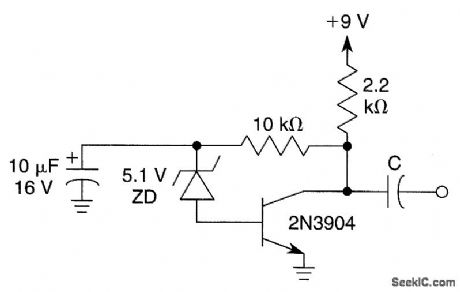
This circuit uses a Zener diode as a noise source. C is chosen to pass the lowest-desired frequency components of the noise. (View)
View full Circuit Diagram | Comments | Reading(3569)
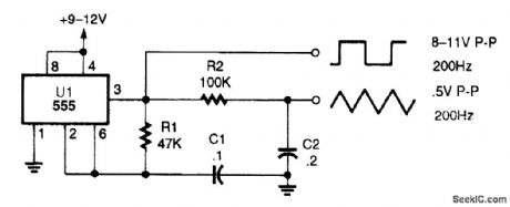
SIMPLE_TEST_SIGNAL_GENERATOR
Published:2009/6/24 22:28:00 Author:May
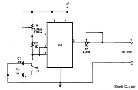
An NE555 generates signals for test purposes. Frequency range is from 20Hz to 10kHz, depending on the setting of S1. +Vis 5 V. (View)
View full Circuit Diagram | Comments | Reading(579)
PULSE_GENERATION_BY_INTERRUPTING_A_LIGHT_BEAM
Published:2009/6/24 22:27:00 Author:May
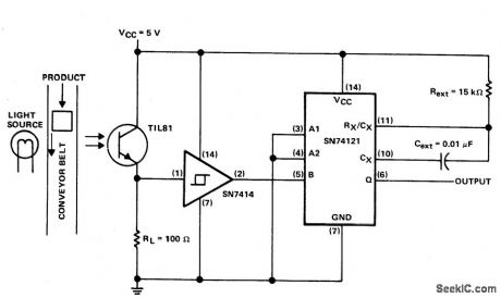
This circuit puts out a pulse when an object on the conveyor belt blocks the light source. The light source keeps the phototran-istor turned on. This produces a high-logic-level voltage at the Schmitt-trigger inverter and a TTL-compatible low logic level at pin 5 of the monostable. When an object blocks the light, TIL81 turns off the Schmitt-trigger inverter to triggers the one shot. (View)
View full Circuit Diagram | Comments | Reading(2216)
DIGITAL_SINE_WAVE_GENERATOR
Published:2009/6/24 22:26:00 Author:May

The sine-wave generator starts with an 8-MHz signal and divides it by eight to obtain 1 MHz at C1 (IC1's 2-MHz and 500-kHz outputs can serve as alternate drive signals). Qllevel-shifts the 1-MHz pulses so that they can drive the bipolar circuitry necessary for producing a bipolar output. Syn-chronous counter IC2 divides 1 MHz by 256 to give the desired output frequency (3906 Hz), and IC3 filters the harmonic frequencies.The filter's clock is taken from the first divide-by-2 tap of IC2 to assure a 50% duty cycle. IC2 fur-ther divides this signal by 128 to ensure that the filter's input signal (1 MHz/256) falls within the flat portion of the filter response.The output of the switched-capacitor filter resembles a sampled sine wave. It can be smoothed by building a first- or second-order low-pass filter around the otherwise uncommitted output op amp. (View)
View full Circuit Diagram | Comments | Reading(2549)
OP_AMP_SAWTOOTH_GENERATOR
Published:2009/6/24 22:25:00 Author:May

The sawtooth generator circuit shown is reset at the end of each cycle. The result is a constant peak-to-peak output throughout the circuit's frequency range.The constant-current generator circuit, the voltage-follower circuit, and the comparator circuit produce the waveform. A 555 timer IC (U2) is configured as a one-shot multivibrator that's triggered by the comparator's negative output pulse. (View)
View full Circuit Diagram | Comments | Reading(1974)
SINE_COSINE_AUDIO_GENERATOR_FOR_GALVANOMETER_EXPERIMENTS_
Published:2009/6/24 22:24:00 Author:May
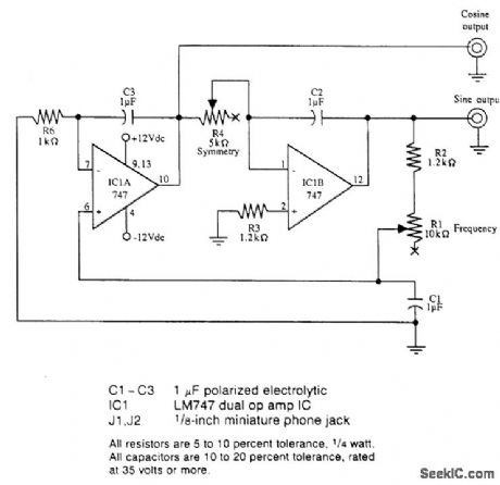
This circuit shows how to implement a sine/cosine audio generator for operating two galvanometers. (View)
View full Circuit Diagram | Comments | Reading(669)
LOW_FREQUENCY_PULSE_GENERATOR
Published:2009/6/24 22:22:00 Author:May
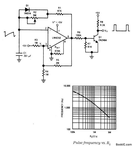
View full Circuit Diagram | Comments | Reading(629)
TRIANGLE_WAVE_GENERATOR_1
Published:2009/6/24 22:22:00 Author:May
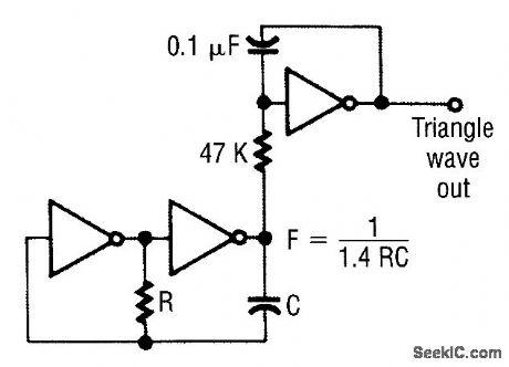
The first two gates are set up as a square-wave oscillator, and the last one makes the conversion to triangle waves. (View)
View full Circuit Diagram | Comments | Reading(789)
TRIANGLE_WAVE_GENERATOR
Published:2009/6/24 22:20:00 Author:May

This oscillator, which is built around an LM1458 dual op amp and a few inexpensive components, produces a 2-V peak-to-peak, triangular waveform. (View)
View full Circuit Diagram | Comments | Reading(0)
SIMPLE_TRIANGLE_WAVEFORM_GENERATOR
Published:2009/6/24 22:19:00 Author:May
The circuit is a triangle waveform-generator circuit that uses as few parts as possible. A 555 timer IC, two resistors, and two capacitors make the triangle waveform. The IC is connected in a 50% duty-cycle astable square-wave oscillator circuit. The square-wave output is fed from pin 3 of the IC to an RC shaping circuit.When the 555's square-wave output goes high, C2 begins to charge through R2 and the voltage across C2 increases as long as the output remains high. When the IC's output goes low again, C2 be-gins to discharge through R2 reducing the voltage across C2 as long as the output remains low. The resulting waveform across C2 takes the shape of a triangle. The best waveform linearity is obtained when R2 and C2 are made as large as possible. With the component values shown, the peak-to-peak output is 0.5 V at a frequency of about 200 Hz. (View)
View full Circuit Diagram | Comments | Reading(2)
SIMPLE_OSCILLOSCOPE_TIMEBASE_GENERATOR
Published:2009/6/24 22:16:00 Author:May
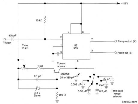
The 555 timer generates both a linear ramp and an output for Z-axis modulations of the CRT electron beam. (View)
View full Circuit Diagram | Comments | Reading(718)
VOLTAGE_CONTROLLED_TWO_PHASE_OSCILLATOR
Published:2009/6/24 22:00:00 Author:May
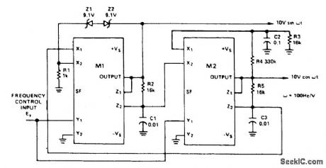
This circuit uses two multipliers for integration-with-contro llable-time -constants in a feedback loop. R2 and R5 will be recognized in the AD534 voltage-to-current configuration; the currents are integrated in C1 and C3, and the voltages they develop are connected at high impedance in proper polarity to the X inputs of the next AD534. The frequency-control input, EY, varies the integrator gains, with a sensitivity of 100 Hz/V, and frequency error typically less than 0.1% of full scale from 0.1V to 10V (10 Hz to 1 kHz). C2 (proportional to C1 and C3), R3, R4 provide regenerative darnp-ing to start and maintain oscillation. Z1 and Z2 stabilize the amplitude at low distortion by degenera-tive damping above ±10V. (View)
View full Circuit Diagram | Comments | Reading(582)
THREE_DECADE_VCO
Published:2009/6/24 21:59:00 Author:May
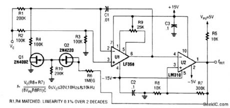
A range of 10 Hz to 10 kHz is covered by this circuit. (View)
View full Circuit Diagram | Comments | Reading(662)
4093_CMOS_VFO
Published:2009/6/24 21:52:00 Author:May

Two gates of a Quad 4093 are used in an astable multivibrator. C1 is a three-gang 365 pF variable capacitor with sections paralleled. S3 and S4 switch in optional extra capacitors. (View)
View full Circuit Diagram | Comments | Reading(2661)
SIMPLE_AUDIO_TEST_OSCILLATOR
Published:2009/6/24 21:50:00 Author:May

An 88-mH surplus telephone toroidal coil is used in a 1-kHz oscillator. Up to 8 V p-p into a high-Z load is available. THD is 0.9%. (View)
View full Circuit Diagram | Comments | Reading(1115)
4093_CMOS_ASTABLE_OSCILLATOR
Published:2009/6/24 21:48:00 Author:May

Two gates of the Quad 4093 are used to make an oscillator. RX can be from about 5 kΩ to around 10 MΩ. CX can be from about 10 pF to many μF, the limit being set by the leakage of the capacitor. Frequency is approximately 2.8/RXCX (R MΩ, Cmfd). (View)
View full Circuit Diagram | Comments | Reading(3791)
SIMPLE_NTSC_GRAY_SCALE_VIDEO_GENERATOR
Published:2009/6/24 21:46:00 Author:May

A 4.032-MHz crystal oscillator (256 x horizontal line scan rate) drives a BCD counter. The binary outputs of the counter are fed to R2 through R5, a simple weighting network for D/A conversion, re-sulting in a staircase video output with a rep rate of 15.75 kHz. This circuit should be useful for am-ateur TV linearity testing and setup purposes. (View)
View full Circuit Diagram | Comments | Reading(2312)
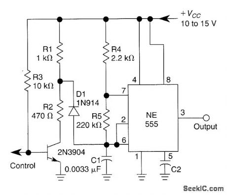
VARIABLE_DUTY_CYCLE_OSCILLATOR
Published:2009/6/24 21:42:00 Author:May

Using a potentiometer and steering diodes, this 1.2-kHz oscillator will provide 1 to 99% duty cycle. Vary C1 to change frequency. (View)
View full Circuit Diagram | Comments | Reading(0)
WIEN_BRIDGE_AUDIO_OSCILLATOR
Published:2009/6/24 21:39:00 Author:May
For variable-frequency operation, R1 and R2 can be replaced by a dual potentiometer. (View)
View full Circuit Diagram | Comments | Reading(603)
PRECISION_GATED_OSCILLATOR
Published:2009/6/24 21:37:00 Author:May
A 1-kHz gated oscillator with no long turn-on cycle is shown. R2, R3, and D1 preset the voltage on tuning capacitor C1 to 1/3 of the supply voltage. (View)
View full Circuit Diagram | Comments | Reading(724)
| Pages:134/195 At 20121122123124125126127128129130131132133134135136137138139140Under 20 |
Circuit Categories
power supply circuit
Amplifier Circuit
Basic Circuit
LED and Light Circuit
Sensor Circuit
Signal Processing
Electrical Equipment Circuit
Control Circuit
Remote Control Circuit
A/D-D/A Converter Circuit
Audio Circuit
Measuring and Test Circuit
Communication Circuit
Computer-Related Circuit
555 Circuit
Automotive Circuit
Repairing Circuit